UPD161622P データシートの表示(PDF) - NEC => Renesas Technology
部品番号
コンポーネント説明
メーカー
UPD161622P Datasheet PDF : 103 Pages
| |||
µ PD161622
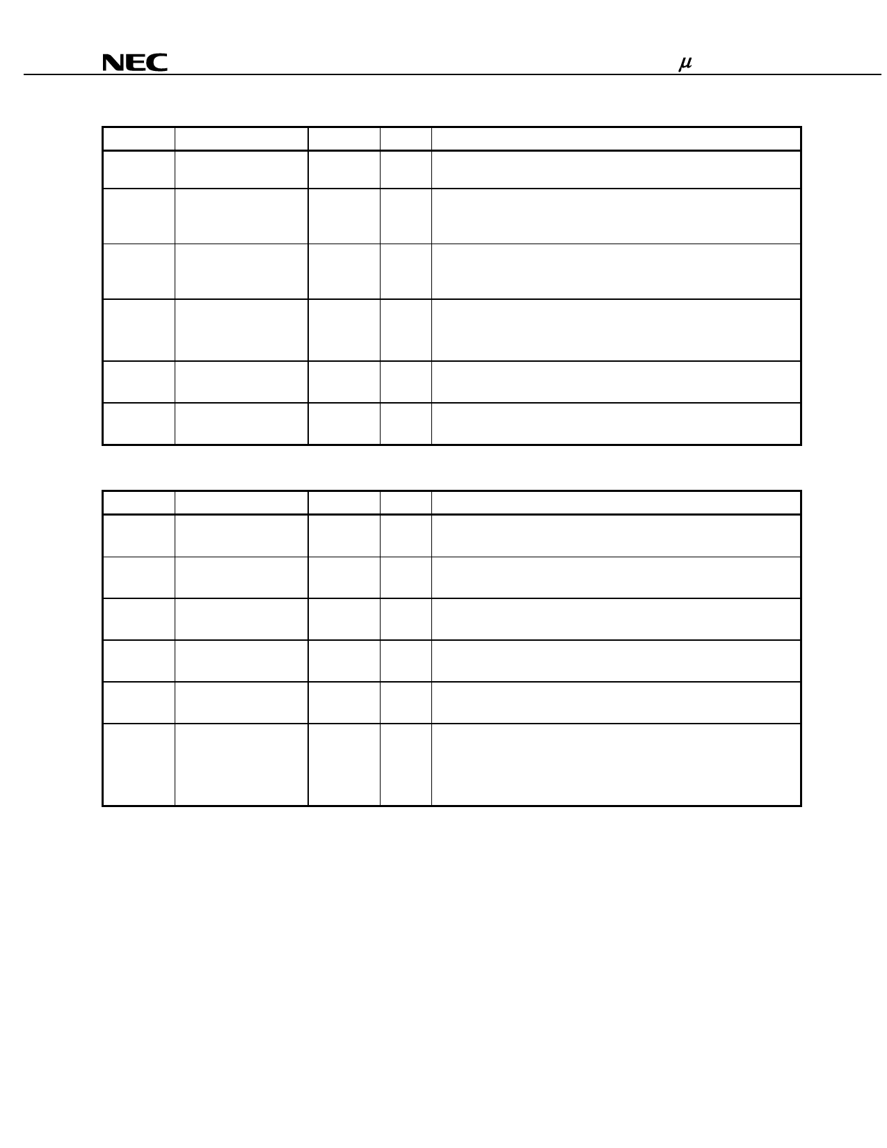
3.3 Gate Driver IC Control Pins
Symbol
Pin Name
Pad No.
LPMG
Low power mode signal 138
GOE1
OE1 output for gate
135
driver
GOE2
OE2 output for gate
136
driver
GSTB
STB output for gate
133
driver
GCLK
CLK output for gate
134
driver
RGONG Regulator control
137
I/O
Function
Output This is an output pin for low power mode (for the gate driver).
Connect to the LPM pin of the gate driver.
Output This pin is an output pin for the low power mode (for the OE1).
Connect to the OE1 pin of the gate driver.
Timing signal for output, refer to 5.4 Display timing generator.
Output This pin is the OE2 output for the gate driver.
Connect to the OE2 pin of the gate driver.
Timing signal for output, refer to 5.4 Display timing generator.
Output This pin is the STB output for the gate driver.
Connect to the STVR or STVL pin of the gate driver.
Timing signal for output, refer to 5.4 Display timing generator.
Output This pin is the CLK output for the gate driver.
Connect to the CLK pin of the gate driver.
Output Regulator ON/OFF control of gate driver IC
Connect to the RGONG pin of the gate driver.
3.4 Power Supply Control Pins
Symbol
Pin Name
Pad No.
LPMP
Low power mode signal 65
DCON
DC/DC converter control 67
RGONP Regulator control
66
VCD11, VCD12 VDD1 booster selection 64, 63
VCD2
VDD2 booster selection 62
VCE
VO level selection
61
I/O
Function
Output Low power mode control signal output pin (for power-supply IC).
This pin connects to LPM pin of power-supply IC.
Output DC/DC converter ON/OFF signal pin for power-supply IC.
This pin connects DCON pin of power-supply IC.
Output Regulator ON/OFF control signal pin for power-supply IC.
This pin connects to RGONP pin of power-supply IC.
Output Control signal to select x4/x5/x6/x7 booster of power-supply IC for VCC1.
Connect to the VCD11 and VCD12 pins of the power-supply IC.
Output Control signal to select x2/x3 booster of power-supply IC for VCC2.
Connect to the VCD2 pin of the power-supply IC.
Output Signal for selecting the level of the power-supply IC booster voltage, to
be used for the maximum voltage of VO. Selects that the booster
voltage level is either the same level as VDD1 or a multiple of minus 1.
Connect to the VCE pin of the power-supply IC.
10
Data Sheet S15649EJ2V0DS
Share Link: 