UPD161623 データシートの表示(PDF) - NEC => Renesas Technology
部品番号
コンポーネント説明
メーカー
UPD161623 Datasheet PDF : 84 Pages
| |||
µ PD161623
(2/2)
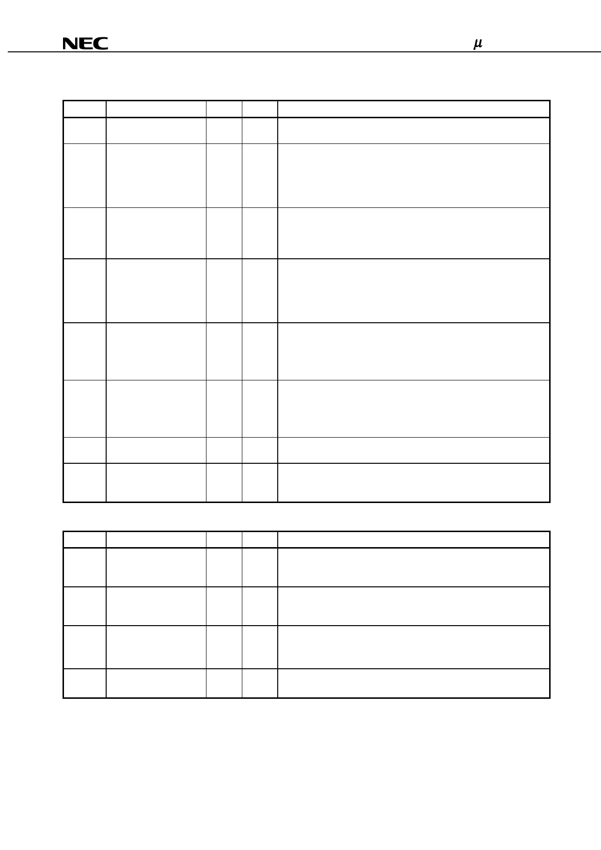
Symbol
Pin Name
D0 to D17 Data bus
RS
Data/command selection
DTX
Data major select
OSCSEL
Oscillation signal
selection
OSCIN
Oscillation signal
OSCOUT Oscillation signal
CSTB
GSTB logic signal
OP0 to
OP7
Output port
Pad No. I/O
Function
67 to 50 I/O These pins comprise 18-bit bi-directional data.
When the chip is not selected, D0 to D17 are in high impedance mode.
71
Input When parallel data transfer has been selected, this pin is usually
connected to the least significant bit of the standard CPU address bus and
is used to distinguish between data from display data and commands.
RS = H: Indicates that data from D0 to D17 is display data.
RS = L: Indicates that data from D0 to D17 is commands.
84
Input When parallel data transfer has been selected, this pin is selected data
major selection that inputs display data through serial interface.
DTX = H: 1-pixel/18-bit mode
DTX = L: 1-pixel/16-bit mode
43
Input This pin is for oscillation signal selection. When is used external resistance
connected oscillation circuit, this pin sets H. When in used CR internal
oscillation circuit, this pin sets L.
OSCSEL = H: External resistance connected oscillation circuit select
OSCSEL = L: CR internal oscillation circuit select
47
Input This pin is for oscillation signal input.
OSCSEL = H: Connect 42 kΩ resistance between OSCIN and OSCOUT.
(240 line, in case of NGO = 0)
OSCSEL = L: Leave it open.
45
Output This pin is for oscillation signal input.
OSCSEL = H: Connect 42 kΩ resistance between OSCIN and OSCOUT.
(240 line, in case of NGO = 0)
OSCSEL = L: Leave it open.
49
Output This pin outputs STB signal for gate driver leveled by interface power
supply voltage (VDD1). This output signal is reverse signal of GSTB.
141 to
148
Output
This is a general-purpose output port. The status of these pins (H or L) can
be write via a command.
Leave open when in unused.
3.3 Gate Driver IC Control Pins
Symbol
GOE1
GOE2
Pin Name
OE1 output for gate driver
OE2 output for gate driver
Pad No.
151
152
I/O
Function
Output This pin is an output pin for the low power mode (for the OE1).
Connect to the OE1 pin of the gate driver.
Timing signal for output, refer to 5.4 Display Timing Generator.
Output This pin is the OE2 output for the gate driver.
Connect to the OE2 pin of the gate driver.
Timing signal for output, refer to 5.4 Display Timing Generator.
GSTB STB output for
149
Output This pin is the STB output for the gate driver.
gate driver
Connect to the STVR or STVL pin of the gate driver.
Timing signal for output, refer to 5.4 Display Timing Generator.
GCLK CLK output for gate driver 150
Output This pin is the CLK output for the gate driver.
Connect to the CLK pin of the gate driver.
Data Sheet S15817EJ2V0DS
9
Share Link: 