UPD75212ACW データシートの表示(PDF) - NEC => Renesas Technology
部品番号
コンポーネント説明
メーカー
UPD75212ACW Datasheet PDF : 70 Pages
| |||
µPD75212A
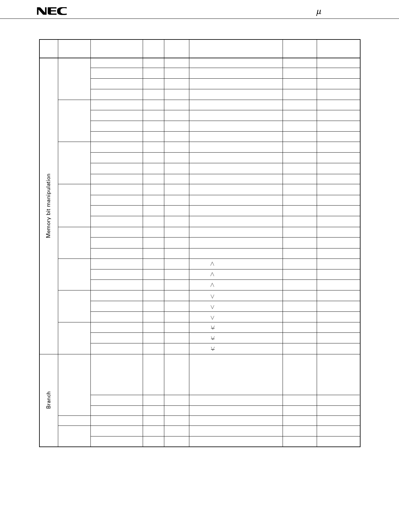
Note Mnemonic
Operands
SET1
CLR1
SKT
SKF
SKTCLR
AND1
OR1
XOR1
BR
mem.bit
fmem.bit
pmem.@L
@H + mem.bit
mem.bit
fmem.bit
pmem.@L
@H+mem.bit
mem.bit
fmem.bit
pmem.@L
@H+mem.bit
mem.bit
fmem.bit
pmem.@L
@H+mem.bit
fmem.bit
pmem.@L
@H+mem.bit
CY, fmem.bit
CY, pmem.@L
CY, @H+mem.bit
CY, fmem.bit
CY, pmem.@L
CY, @H+mem.bit
CY, fmem.bit
CY, pmem.@L
CY, @H+mem.bit
addr
BRCB
BR
!addr
$addr
!caddr
PCDE
PCXA
No. of Machine
Bytes Cycle
Operation
Addressing
Area
Skip
Condition
2
2
(mem.bit)←1
*3
2
2
(fmem.bit)←1
*4
2
2
(pmem7–2+L3–2.bit(L1–0))←1
*5
2
2
(H+mem3–0.bit)←1
*1
2
2
(mem.bit)←0
*3
2
2
(fmem.bit)←0
*4
2
2
(pmem7–2+L3–2.bit(L1–0))←0
*5
2
2
(H+mem3–0.bit)←0
*1
2
2 + S Skip if (mem.bit) = 1
*3
(mem.bit) = 1
2
2 + S Skip if (fmem.bit) = 1
*4
(fmem.bit) = 1
2
2 + S Skip if (pmem7–2+L3–2.bit(L1–0)) = 1
*5
(pmem.@L) = 1
2
2 + S Skip if (H+mem3–0.bit) = 1
*1
(@H+mem.bit) = 1
2
2 + S Skip if (mem.bit) = 0
*3
(mem.bit) = 0
2
2 + S Skip if (fmem.bit) = 0
*4
(fmem.bit) = 0
2
2 + S Skip if (pmem7–2+L3–2.bit(L1–0)) = 0
*5
(pmem.@L) = 0
2
2 + S Skip if (H+mem3–0.bit) = 0
*1
(@H+mem.bit) = 0
2
2 + S Skip if (fmem.bit) = 1 and clear
*4
(fmem.bit) = 1
2
2 + S Skip if (pmem7–2+L3–2.bit(L1–0))=1 and clear
*5
(pmem.@L) = 1
2
2 + S Skip if (H+mem3–0.bit)=1 and clear
*1
(@H+mem.bit)=1
2
2
CY←CY (fmem.bit)
*4
2
2
CY←CY (pmem7–2+L3–2.bit(L1–0))
*5
2
2
CY←CY (H+mem3–0.bit)
*1
2
2
CY←CY (fmem.bit)
*4
2
2
CY←CY (pmem7–2+L3–2.bit(L1–0))
*5
2
2
CY←CY (H+mem3–0.bit)
*1
2
2
CY←CY (fmem.bit)
*4
2
2
CY←CY (pmem7–2+L3–2.bit(L1–0))
*5
2
2
CY←CY (H+mem3–0.bit)
*1
—
—
PC13–0←addr
*6
(Optimum instruction is
selected from among BR !addr,
BRCB !caddr and BR $addr by an
assembler.)
3
3
PC13–0←addr
*6
1
2
PC13–0←addr
*7
2
2
PC13–0←PC13,12+caddr11–0
*8
2
3
PC13–0←PC13–8+DE
2
3
PC13–0←PC13–8+XA
Note Instruction Group
40
Share Link: 