UPD75P0016CU データシートの表示(PDF) - NEC => Renesas Technology
部品番号
コンポーネント説明
メーカー
UPD75P0016CU Datasheet PDF : 60 Pages
| |||
µPD75P0016
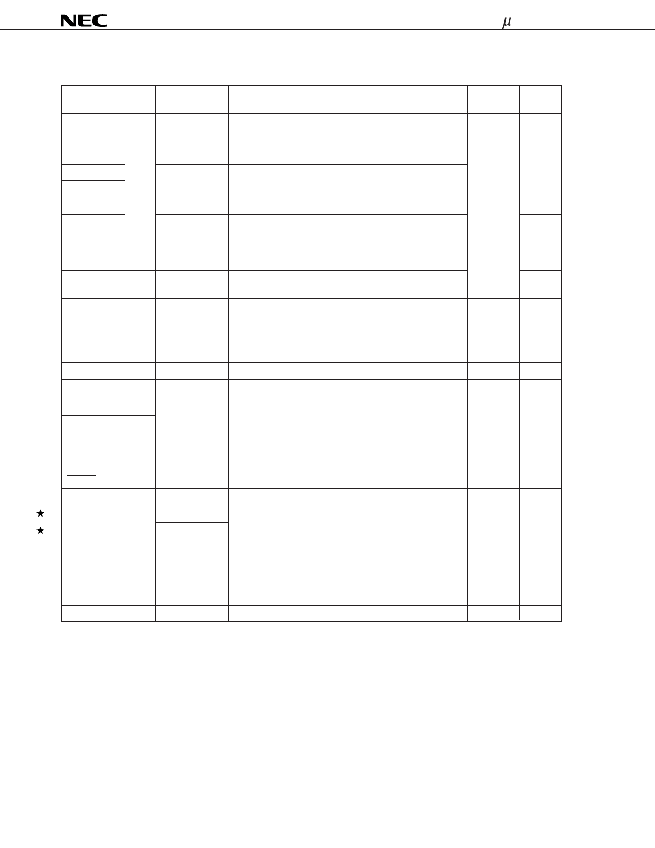
3.2 Non-port Pins
Pin name
I/O
Shared by
Function
When
reset
TI0
PTO0
PTO1
I P13
O P20
P21
External event pulse input to timer/event counter
Timer/event counter output
Timer counter output
Input
Input
PCL
BUZ
P22
Clock output
P23
Outputs any frequency (for buzzer or system clock trimming)
SCK
SO/SB0
I/O P01
P02
Serial clock I/O
Serial data output
Serial data bus I/O
Input
SI/SB1
P03
Serial data input
Serial data bus I/O
INT4
INT0
INT1
I P00
I P10
P11
Edge-triggered vectored interrupt input
(Detects both rising and falling edges).
Edge-triggered vectored interrupt input
(detected edge is selectable).
INT0/P10 can select noise elimination
circuit.
With noise eliminator
/asynch selectable
Asynch
Input
INT2
KR0-KR3
KR4-KR7
P12
I P60-P63
I P70-P73
Rising edge-triggered testable input
Falling edge-triggered testable input
Falling edge-triggered testable input
Asynch
Input
Input
X1
X2
XT1
XT2
RESET
MD0-MD3
I—
—
I—
—
I—
I P30-P33
Ceramic/crystal resonator connection for main system clock.
If using an external clock, input it to X1 and input the
inverted clock to X2.
Crystal resonator connection for subsystem clock.
If using an external clock, input it to XT1 and input the invert-
ed clock to X2. XT1 can be used as a 1-bit (test) input.
System reset input (low level active)
Mode selection for program memory (PROM) write/verify.
—
—
—
Input
D0-D3
D4-D7
VPP Note 2
I/O P40-P43
P50-P53
——
Data bus pin for program memory (PROM) write/verify.
Input
Programmable voltage supply in program memory (PROM)
—
write/verify mode.
In normal operation mode, connect directly to VDD.
Apply +12.5 V in PROM write/verify mode.
VDD
——
Positive power supply
—
VSS
——
Ground potential
—
Notes 1. Circuit types enclosed in brackets indicate Schmitt triggered inputs.
2. During normal operation, the VPP pin will not operate normally unless connected to VDD pin.
I/O circuit
type Note 1
<B>-C
E-B
<F>-A
<F>-B
<M>-C
<B>
<B>-C
<F>-A
<F>-A
—
—
<B>
E-B
M-E
—
—
—
8
Data Sheet U10328EJ3V1DS00
Share Link: 