UPG100B データシートの表示(PDF) - NEC => Renesas Technology
部品番号
コンポーネント説明
メーカー
UPG100B Datasheet PDF : 4 Pages
| |||
UPG100B, UPG100P
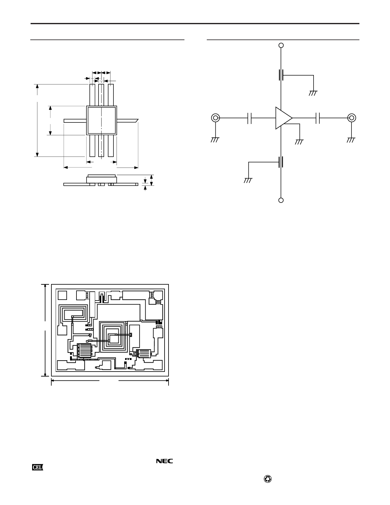
OUTLINE DIMENSIONS (Units in mm)
UPG 100B
PACKAGE OUTLINE B08
1.27±0.1 1.27±0.1
(LEADS 2, 4, 6, 8) 0.6
10.6 MAX
0.4 (LEADS 1, 3, 5, 7)
43 2
5
1
3.8±0.2
678
3.8±0.2
10.6 MAX
LEAD CONNECTIONS:
1. INPUT
5. OUTPUT
2. GND
6. GND
3. VGG
7. VDD
4. GND
8. GND
1.7 MAX
0.2
+0.05
-0.02
TEST CIRCUIT
VDD
1000 pF
7
IN
100 pF*
100 pF*
OUT
1
5
3
2, 4, 6, 8
1000 pF**
VGG
* Chip Capacitor
**Recommended when cascading UPG100 with NEC's UPG100, 101,
103B's.
UPG100P (CHIP)
GND
VDD
GND
1.0 mm
IN
OUT
GND GND
VGG
1.3 mm
GND
Notes: Bonding Pad Size: 100 µm Square
Distance between Bonding Pad Outer Edge and Die Edge:
70 µm Typical
Chip Thickness: 140± 10 µm
RECOMMENDED CHIP ASSEMBLY CONDITIONS
DIE ATTACHMENT
Atmosphere: N2 gas
Temperature: 320± 5°C
AuSn Preform: 0.5 x 0.5 x 0.05t (mm), 1 piece
The hard solder such as AuSi or AuGe which has
higher melting point than AuSn should not be used.
Epoxy Die Attach is not recommended.
Base Material: CuW, Cu, Kovar (Other material should not be used)
BONDING
Machine:
Thermo-compression bonding. Ultrasonic bonding is
not recommended.
Wire:
30 µm diameter Au wire, 10 wires
Temperature: 260 ± 5°C
Strength:
31 ± 3g
Atmosphere: N2 gas
It is critical that GND points be connected to the ground with
the shortest possible wire.
EXCLUSIVE NORTH AMERICAN AGENT FOR
RF, MICROWAVE & OPTOELECTRONIC SEMICONDUCTORS
CALIFORNIA EASTERN LABORATORIES • Headquarters • 4590 Patrick Henry Drive • Santa Clara, CA 95054-1817 • (408) 988-3500 • Telex 34-6393 • FAX (408) 988-0279
24-Hour Fax-On-Demand: 800-390-3232 (U.S. and Canada only) • Internet: http://WWW.CEL.COM
DATA SUBJECT TO CHANGE WITHOUT NOTICE
PRINTED IN USA ON RECYCLED PAPER -10/97
Share Link: 