VN3205 データシートの表示(PDF) - Supertex Inc
部品番号
コンポーネント説明
メーカー
VN3205 Datasheet PDF : 4 Pages
| |||
Thermal Characteristics
Package
TO-92
ID (continuous)*
1.2A
ID (pulsed)
8.0A
Power Dissipation
@ TC = 25°C
1.0W
θjc
°C/W
125
SOT-89
Plastic DIP
1.5A
1.5A
8.0A
8.0A
1.6W (TA = 25°C)
3.0W‡
15
41.6‡
* ID (continuous) is limited by max rated Tj. TA = 25°C.
† Mounted on FR5 board, 25mm x 25mm x 1.57mm. Significant PD increase possible on ceramic substrate.
‡ Total for package.
θja
°C/W
170
78†
83.3‡
IDR*
1.2A
1.5A
1.5A
VN3205
IDRM
8.0A
8.0A
8.0A
Electrical Characteristics (@ 25°C unless otherwise specified)
Symbol
Parameter
Min Typ Max Unit
BVDSS
VGS(th)
∆VGS(th)
IGSS
IDSS
Drain-to-Source Breakdown Voltage
Gate Threshold Voltage
Change in VGS(th) with Temperature
Gate Body Leakage
Zero Gate Voltage Drain Current
50
V
0.8
2.4
V
-4.3 -5.5 mV/°C
1 100
nA
10
µA
1
mA
ID(ON)
ON-State Drain Current
3.0
14
A
RDS(ON)
Static Drain-to-Source TO-92 and P-DIP
ON-State Resistance SOT-89
0.45
Ω
0.45
Ω
TO-92 and P-DIP
0.3
Ω
SOT-89
0.3
Ω
∆RDS(ON) Change in RDS(ON) with Temperature
0.85
1.2 %/°C
GFS
Forward Transconductance
1.0
1.5
CISS
Input Capacitance
220 300
COSS
Common Source Output Capacitance
70 120
pF
CRSS
Reverse Transfer Capacitance
20
30
td(ON)
Turn-ON Delay Time
10
tr
Rise Time
15
ns
td(OFF)
Turn-OFF Delay Time
25
tf
Fall Time
25
VSD
Diode Forward Voltage Drop
1.6
V
trr
Reverse Recovery Time
300
ns
Notes:
1. All D.C. parameters 100% tested at 25°C unless otherwise stated. (Pulse test: 300µs pulse, 2% duty cycle.)
2. All A.C. parameters sample tested.
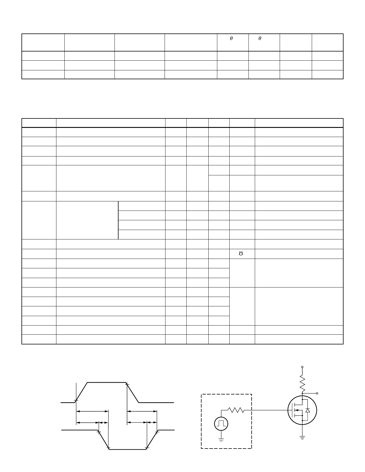
Switching Waveforms and Test Circuit
10V
INPUT
0V 10%
t(ON)
90%
t(OFF)
td(ON)
tr
td(OFF)
tF
VDD
OUTPUT
0V
10%
90%
10%
90%
PULSE
GENERATOR
Rgen
INPUT
2
Conditions
VGS = 0V, ID = 10mA
VGS = VDS, ID = 10mA
VGS = VDS, ID = 10mA
VGS = ±20V, VDS = 0V
VGS = 0V, VDS = Max Rating
VGS = 0V, VDS = 0.8 Max Rating
TA = 125°C
VGS = 10V, VDS = 5V
VGS = 4.5V, ID = 1.5A
VGS = 4.5V, ID = 0.75A
VGS = 10V, ID = 3A
VGS = 10V, ID = 1.5A
VGS = 10V, ID = 3A
VDS = 25V, ID = 2A
VGS = 0V, VDS = 25V
f = 1 MHz
VDD = 25V
ID = 2A
RGEN = 10Ω
VGS = 0V, ISD = 1.5A
VGS = 0V, ISD = 1A
VDD
RL
OUTPUT
D.U.T.
Share Link: 