VSC7139 データシートの表示(PDF) - Vitesse Semiconductor
部品番号
コンポーネント説明
メーカー
VSC7139 Datasheet PDF : 18 Pages
| |||
VITESSE
SEMICONDUCTOR CORPORATION
Quad Transceiver for
Gigabit Ethernet and Fibre Channel
Preliminary Datasheet
VSC7139
Functional Description
Notation
In this document, each of the four channels are identified as Channel A, B, C or D. When discussing a sig-
nal on any specific channel, the signal will have the Channel letter embedded in the name, i.e., “TA(0:9).” When
referring to the common behavior of a signal which is used on each of the four channels, a lower case “x” is
used in the signal name, i.e. Tx(0:9). Differential signals, i.e. RA+ and RA-, may be referred to as a single sig-
nal, i.e. RA, by dropping reference to the “+” and “-”. “REF” refers to either the TTL input REFT, or the PECL
differential inputs REF+/REF-, whichever is used.
Clock Synthesizer
The VSC7139 clock synthesizer multiplies the reference frequency provided on the REF input by 10 or 20
to achieve a baud rate clock between 1.05GHz and 1.36GHz. The REF input can be either TTL or PECL. If
TTL, connect the TTL input clock to REFT. If PECL, connect the PECL inputs to REF+ and REF-. The internal
clock presented to the Clock Synthesizer is a logical XNOR of REFT and REF+/-. The reference clock will be
active HIGH if the unused input is HIGH. The reference clock is active LOW if the unused input is LOW. REFT
has an internal pull-up resistor. Internal biasing resistors set the proper DC level on REF+/- so AC-coupling may
be used.
The TTL outputs, RFCO0 and RFCO1, provide a clock that is frequency locked to the REF input. This
clock is derived from the clock synthesizer and is always 1/10 the baud rate, regardless of the state of the RFCM
input.
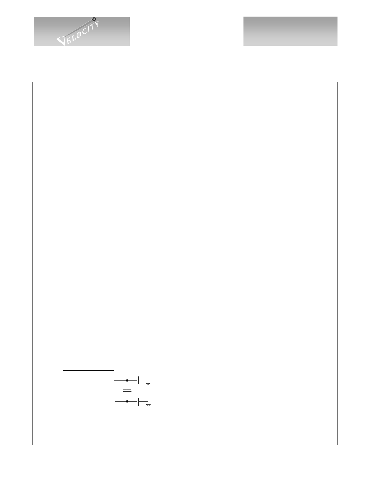
The on-chip PLL uses a single external 0.1µF capacitor, connected between CAP0 and CAP1, to control the
Loop Filter. This capacitor should be a multilayer ceramic dielectric, or better, with at least a 5V working
voltage rating and a good temperature coefficient, i.e., NPO is preferred but X7R may be acceptable. These
capacitors are used to minimize the impact of common mode noise on the Clock Multiplier Unit (CMU),
especially power supply noise. Higher value capacitors provide better robustness in systems. NPO is preferred
because if an X7R capacitor is used, the power supply noise sensitivity will vary with temperature.
For best noise immunity, the designer may use a three capacitor circuit with one differential capacitor
between CAP0 and CAP1, C1, a capacitor from CAP0 to ground, C2, and a capacitor from CAP1 to ground,
C3. Larger values are better but 0.1µF is adequate. However, if the designer cannot use a three capacitor circuit,
a single differential capacitor, C1, is adequate. These components should be isolated from noisy traces.
Figure 1: Loop Filter Capacitors (Best Circuit)
C2
CAP0
VSC7139
C1
CAP1
C3
C1=C2=C3= >0.1µF
MultiLayer Ceramic
Surface Mount
NPO (Preferred) or X7R
5V Working Voltage Rating
Page 2
© VITESSE SEMICONDUCTOR CORPORATION • 741 Calle Plano • Camarillo, CA 93012
Tel: (800) VITESSE • FAX: (805) 987-5896 • Email: prodinfo@vitesse.com
Internet: www.vitesse.com
G52196-0, Rev 3.3
5/14/01
Share Link: 