VSC7969 データシートの表示(PDF) - Vitesse Semiconductor
部品番号
コンポーネント説明
メーカー
VSC7969
Vitesse Semiconductor

VSC7969 Datasheet PDF : 14 Pages
| |||
VITESSE
SEMICONDUCTOR CORPORATION
Advance Product Information
VSC7969
3.125Gb/s Integrated Transimpedance
and Limiting Amplifier with Signal Detect
Features
• Integrated TIA and Limiting Amplifier
• Low Power Consumption for SFF Applications
• TO Package-Compatible Layout
• On-Chip Signal Detect
• On-Chip Linear Photocurrent Monitor
• Single 3.3V Supply
• 5V Supply Operation via Wirebond Option
• Compatible with PIN or Avalanche Detectors
• Packages: 16-Pin TSSOP, TO-46, Bare Die
Applications
• 2.488Gb/s, 3.125Gb/s SONET OC-48/
SDH STM-16
• 2.125Gb/s Fibre Channel
• 2.5Gb/s or 3.125Gb/s Ethernet Applications with
8B/10B Overhead
• SFF Transceivers
General Description
The VSC7969 is a 3.125Gb/s transimpedance amplifier IC with a built-in limiting amplifier, a signal detect
feature and a photocurrent monitor. The VSC7969 does not require any external electrical components in the
construction of a high performance optical receiver such as for SONET/SDH applications. The analog output is
a differential signal with a minimum amplitude of 200mVp-p (single-ended). The VSC7969 operates with a sin-
gle power supply with a maximum power dissipation of 300mW. A PIN photodiode or APD can be connected
and separately biased to provide optimal performance.
The VSC7969 provides filtered bias for MSM and PIN photodetectors; applications using an APD photode-
tector must supply bias separately. The VSC7969 also provides a photocurrent monitor whose output is linearly
proportional to the input photocurrent.
The VSC7969 can operate from a single +3.3V supply or a +5V or -5.2V supply. The VSC7969 is offered
in die form and in a 16-pin plastic thin-shrink small outline package (TSSOP-16). A fully tested TO-46 outline
packaged receiver with a photodetector is also available.
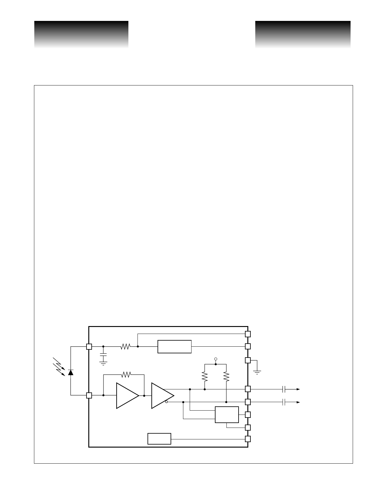
Block Diagram
Filter
In
VSC7969
+3.3V
+5V
Regulator
+3.3V
50Ω
50Ω
Monitor
Signal
Detect
VCCS
VCCD
Dual power supply pins are
provided for +5V or +3.3V
operation. Only one power
supply pin should be connected.
GND
VOUTP
Outputs need to
be AC-coupled
VOUTN 0.1µF
0.1µF
SD_OUT
SD_ADJ
IMON
G52355-0, Rev 2.0
02/09/01
© VITESSE SEMICONDUCTOR CORPORATION • 741 Calle Plano • Camarillo, CA 93012
Tel: (800) VITESSE • FAX: (805) 987-5896 • Email: prodinfo@vitesse.com
Internet: www.vitesse.com
Page 1
Share Link: