VSX60MD35U データシートの表示(PDF) - C AND D TECHNOLOGIES
部品番号
コンポーネント説明
メーカー
VSX60MD35U Datasheet PDF : 4 Pages
| |||
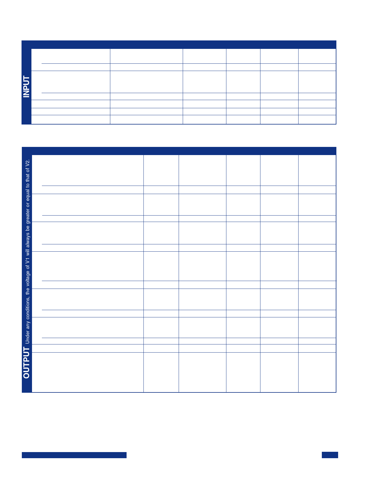
SPECIFICATIONS, ALL MODELS
Specifications are at TCASE = +40°C nominal input voltage unless otherwise specified.
PARAMETER
Operating Input Voltage
VSX60LD
VSX60MD
Maximum Input Current
(Vi=0V to Vi max, Io=Io max)
VSX60LD
VSX60MD
I/P Reflected Ripple Current
No Load Input Current
On/Off Activated Input Current
SYMBOL
Vi
Vi
Ii max
Ii max
IiNL
IiQ
MIN
TYP
18
24
36
48
50
17
MAX
36
75
5.0
2.25
400
UNITS
VDC
VDC
A
A
mA p-p
mA
mA
PARAMETER
Output voltage
( Over all conditions of I/P voltage, load
and temperature)
3.3 Vout (V2)
5.0 Vout (V1)
Output Voltage Setpoint
(Vi=48, Io3=9A, Io5=6A, Tc=25°C)
3.3 Vout (V2)
5.0 Vout (V1)
Output Ripple and Noise Voltage
(peak-to-peak, 100 MHz BW)
3.3 Vout (V2)
5.0 Vout (V1)
Output Current
(Total module O/P power should not
exceed 60 Watts)
3.3 Vout (V2)
5.0 Vout (V1)
Output Current Limit Inception
(Vo=95% of Vo nom)
3.3 Vout (V2)
5.0 Vout (V1)
Output Short Ckt Current
(Max impedance across short circuit = 65mΩ)
3.3 Vo
5.0 Vo
Efficiency (Vi=48V, Io3=9A,Io5=6A, Tc=70°C)
Dynamic Response (∆Io/∆t=0.2A/µsec.
Vi=48V, Tc=25°C, either O/P)
Load change of 50% Io max; at any
operating load up to Iomax or Pomax
Peak Deviation outside settling point
SYMBOL
3.3 Vo
5.0 Vo
3.3 Vo,set
5.0 Vo,set
_
_
Io3
Io5
Io3cli
Io5cli
η
–
MIN
3.2
4.8
3.26
4.96
_
_
_
_
19.0
12.5
16
16
11
89
–
TYP
MAX
UNITS
_
3.4
Vdc
_
5.2
Vdc
3.30
3.34
Vdc
5.02
5.08
Vdc
_
60
mv p-p
_
80
mv p-p
_
15
A
_
12
A
21.0
23.0
A
13.5
15.0
A
19
22
A
19
22
A
14
17
A
90
_
%
2
_
%Vo nom
Product: www.cdpowerelectronics.com
VSX60xD35 REV D 5/02
2
Share Link: 