W91330N データシートの表示(PDF) - Winbond
部品番号
コンポーネント説明
メーカー
W91330N Datasheet PDF : 17 Pages
| |||
W91330N SERIES
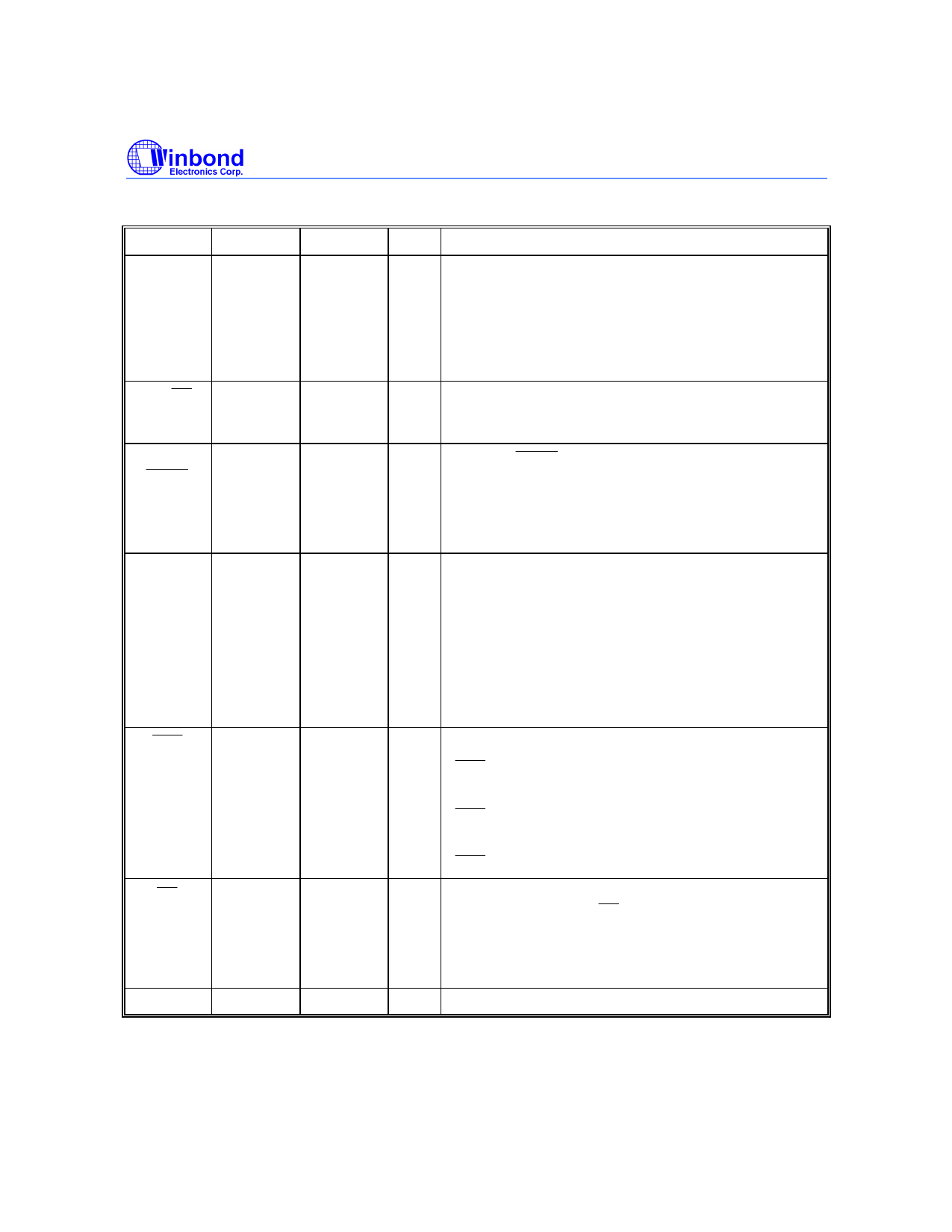
PIN DESCRIPTION
SYMBOL 18-PIN
Column-
Row
Inputs
1−4
&
15−18
XT, XT
7, 8
T/P
9
MUTE
MODE
13
HKS
10
DP
11
VDD, VSS
14, 6
20-PIN
1−4
&
17−20
7, 8
9
15
12
13
16, 6
I/O
FUNCTION
The keyboard inputs may be used with either the
I
standard 5 × 4 keyboard or the inexpensive single
contact (Form A) keyboard. Electronic input from a
µC can also be used.
A valid key-in is defined as a single row being
connected to a single column.
I, O A built-in inverter provides oscillation with an
inexpensive 3.579545 MHz crystal or ceramic
resonator.
O The T/P MUTE is a conventional CMOS N-channel
open drain output.
The output transistor is switched on during dialing
sequence, one-key redial break, and flash break
time. Otherwise, it is switched off.
I Pulling mode pin to VSS places the dialer in tone
mode.
Pulling mode pin to VDD places the dialer in pulse
mode. (10 ppS; 20 ppS for W91331N/W91331AN,
M/B = 40:60)
Floating mode pin places the dialer in pulse mode.
(10 ppS; 20 ppS for W91331N/W91331AN, M/B =
33.3:66.7).
I Hook switch input.
HKS = VDD: On-hook state. Chip in sleeping mode,
no operation.
HKS = VSS: Off-hook state. Chip enabled for normal
operation.
HKS pin is pulled to VDD by internal resistor.
O N-channel open drain dialing pulse output.
Flash key will cause DP to be active in either tone
mode or pulse mode.
The timing diagram for pulse mode is shown in
Figure 1(a, b, c, d).
I Power input pins.
Publication Release Date: May 1997
-3-
Revision A2
Share Link: 