WFF840 データシートの表示(PDF) - Wisdom technologies
部品番号
コンポーネント説明
メーカー
WFF840 Datasheet PDF : 7 Pages
| |||
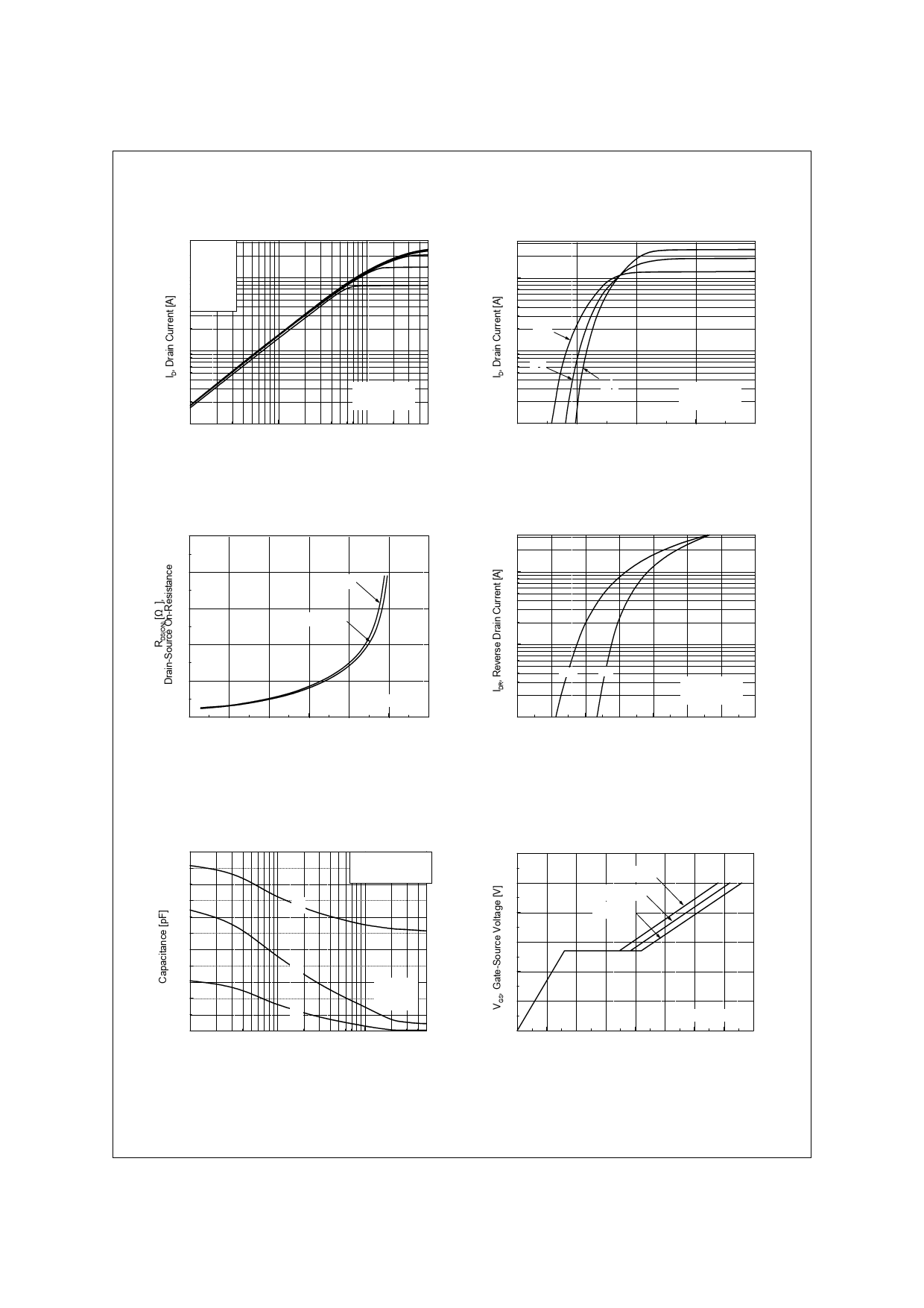
Typical Characteristics
Top : 15V.0GSV
10.0 V
8.0 V
101
7.0 V
6.5 V
6.0 V
5.5 V
Bottom : 5.0 V
100
10-1
10-1
※ Notes :
1. 250µs Pulse Test
2. TC = 25℃
100
101
VDS, Drain-Source Voltage [V]
Figure 1. On-Region Characteristics
3.0
2.5
VGS = 10V
2.0
VGS = 20V
1.5
1.0
※ Note : TJ = 25℃
0.5
0
5
10
15
20
25
30
ID, Drain Current [A]
Figure 3. On-Resistance Variation vs
Drain Current and Gate Voltage
2500
2000
1500
C = C + C (C = shorted)
iss
gs
gd ds
Coss = Cds + Cgd
Crss = Cgd
Ciss
1000
500
0
10-1
Coss
※ Notes :
1. VGS = 0 V
Crss
2. f = 1 MHz
100
101
VDS, Drain-Source Voltage [V]
Figure 5. Capacitance Characteristics
101
150oC
100
25oC
10-1
2
-55oC
※ Notes :
1. VDS = 40V
2. 250µ s Pulse Test
4
6
8
10
VGS, Gate-Source Voltage [V]
Figure 2. Transfer Characteristics
101
100
10-1
0.2
150℃ 25℃
※ Notes :
1. VGS = 0V
2. 250µ s Pulse Test
0.4
0.6
0.8
1.0
1.2
1.4
1.6
VSD, Source-Drain voltage [V]
Figure 4. Body Diode Forward Voltage
Variation with Source Current
and Temperature
12
VDS = 100V
10
VDS = 250V
8
VDS = 400V
6
4
2
※ Note : ID = 8 A
0
0
5
10
15
20
25
30
35
40
QG, Total Gate Charge [nC]
Figure 6. Gate Charge Characteristics
Share Link: 