WM2619 データシートの表示(PDF) - Wolfson Microelectronics plc
部品番号
コンポーネント説明
メーカー
WM2619 Datasheet PDF : 9 Pages
| |||
Production Data
WM2619
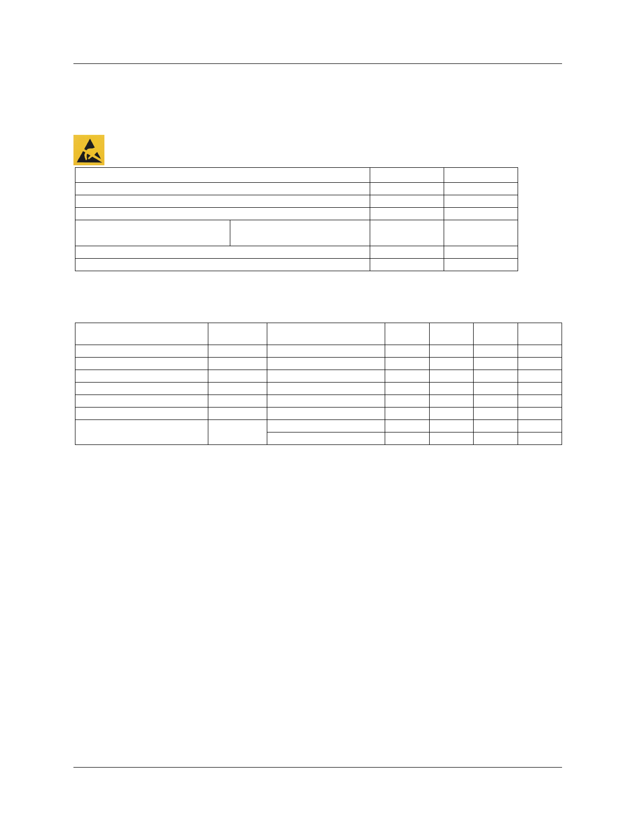
ABSOLUTE MAXIMUM RATINGS
Absolute Maximum Ratings are stress ratings only. Permanent damage to the device may be caused by continuously
operating at or beyond these limits. Device functional operating limits and guaranteed performance specifications are given
under Electrical Characteristics at the test conditions specified.
ESD Sensitive Device. This device is manufactured on a CMOS process. It is therefore generically
susceptible to damage from excessive static voltages. Proper ESD precautions must be taken during
handling and storage of this device
CONDITION
MIN
MAX
Digital Supply voltage, VDD to GND
Reference input voltage
Digital input voltages
Operating temperature range, TA
WM2619C
WM2619I
-0.3V
-0.3V
0°C
-40°C
7V
VDD + 0.3V
VDD + 0.3V
70°C
85°C
Storage temperature
Lead temperature 1.6mm (1/16 inch) soldering for 10 seconds
-65°C
150°C
260°C
RECOMMENDED OPERATING CONDITIONS
PARAMETER
SYMBOL
TEST CONDITIONS
MIN
TYP
Supply voltage
VDD
2.7
High-level digital input voltage
VIH
VDD = 2.7V to 5.5V
2
Low-level digital input voltage
VIL
VDD = 2.7V to 5.5V
Reference voltage to REFIN
VREF
See Note
Load resistance
RL
2
10
Load capacitance
CL
Operating free-air temperature
TA
WM2619C
0
WM2619I
-40
Note: Reference input voltages greater than VDD/2 will cause output saturation for large DAC codes.
MAX
5.5
0.8
VDD - 1.5
100
70
85
UNIT
V
V
V
V
kΩ
pF
°C
°C
WOLFSON MICROELECTRONICS LTD
Production Data Rev1.0 June 1999
3
Share Link: 