WM8143-12 データシートの表示(PDF) - Wolfson Microelectronics plc
部品番号
コンポーネント説明
メーカー
WM8143-12 Datasheet PDF : 24 Pages
| |||
WM8143-12
Production Data
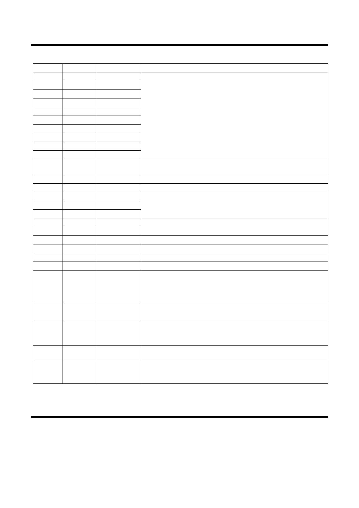
Pin Description
PIN
NAME
1
OP[2]
2
OP[3]
3
OP[4]
4
OP[5]
5
OP[6]
6
OP[7]
7
OP[8]
8
OP[9]
9
OP[10]
10
OP[11]
11
NRESET
12
AVDD
13
AGND
14
VRU
15
VRB
16
VRT
17
VMID
18
VRLC
19
BINP
20
GINP
21
RINP
22
OEB
23
SEN/STB
24
SDI/DNA
25
SCK/RNW
26
RLC
27
VSMP
TYPE
Digital OP
Digital OP
Digital IO
Digital IO
Digital IO
Digital IO
Digital IO
Digital IO
Digital IO
Digital IO
Digital IP
Analogue supply
Analogue supply
Analogue IP
Analogue OP
Analogue OP
Analogue OP
Analogue OP
Analogue IP
Analogue IP
Analogue IP
Digital IP
Digital IP
Digital IP
Digital IP
Digital IP
Digital IP
DESCRIPTION
Tri-state digital 12-bit bi-directional bus. There are four modes:
Tri-state:
when OEB = 1
Output twelve-bit:
twelve bit data is output from bus
Output 8-bit multiplexed:
data output on OP[11:4] at 2 * ADC
conversion Rate
Input 8-bit:
control data is input on bits OP[11:4] in
parallel mode when SCK/RNW = 0.
MSB of the output word is OP[11], LSB is OP[0]
Reset input, active low. This signal forces a reset of all internal registers and selects
whether the serial control bus or parallel control bus is used (see SEN/STB)
Positive analogue supply (5V)
Analogue ground (0V)
ADC reference voltages. The ADC reference range is applied between VRT (full
scale) and VRB (zero level). VRU can be used to derive optimal reference voltages
from an external 5V reference
Buffered mid-point of ADC reference string
Selectable analogue output voltage for RLC
Blue channel input video
Green channel input video
Red channel input video
Output tri-state control:
all outputs enabled when OEB = 0
Serial interface:
enable, active high
Parallel interface:
strobe, active low
Latched on NRESET rising edge: If low then device control is by serial interface, if
high then device control is by parallel interface
Serial interface:
serial interface input data signal
Parallel interface:
high = data, low = address
Serial interface:
serial interface clock signal
Parallel interface:
high = OP[11:4] is output bus
low = OP[11:4] is input bus
Selects whether reset level clamp is applied on a pixel-by-pixel basis. If RLC is
required on each pixel then this pin can be tied high
Video sample synchronisation pulse. This signal is applied synchronously with
MLCK to specify the point in time that the input is sampled. The timing of internal
multiplexing between the R, G and B channels is derived from this signal.
Wolfson Microelectronics
6
PD. Rev 4 Nov 99
Share Link: 