WM8143-12 データシートの表示(PDF) - Wolfson Microelectronics plc
部品番号
コンポーネント説明
メーカー
WM8143-12 Datasheet PDF : 24 Pages
| |||
WM8143-12
System Description
COLOUR CCD
SENSOR
BUFFERING
FOR CCD
RED
GREEN
RINP
OP[11:0]
WM8143-12
GINP
OEB
SDI/DNA
SCK/RNW
SEN/STB
NRESET
BLUE
BINP
VSMP
MCLK
RLC
Production Data
PARALLEL
DATA I/O
CONTROL/SERIAL
DATA IN
ANALOGUE
INTERFACE TIMING
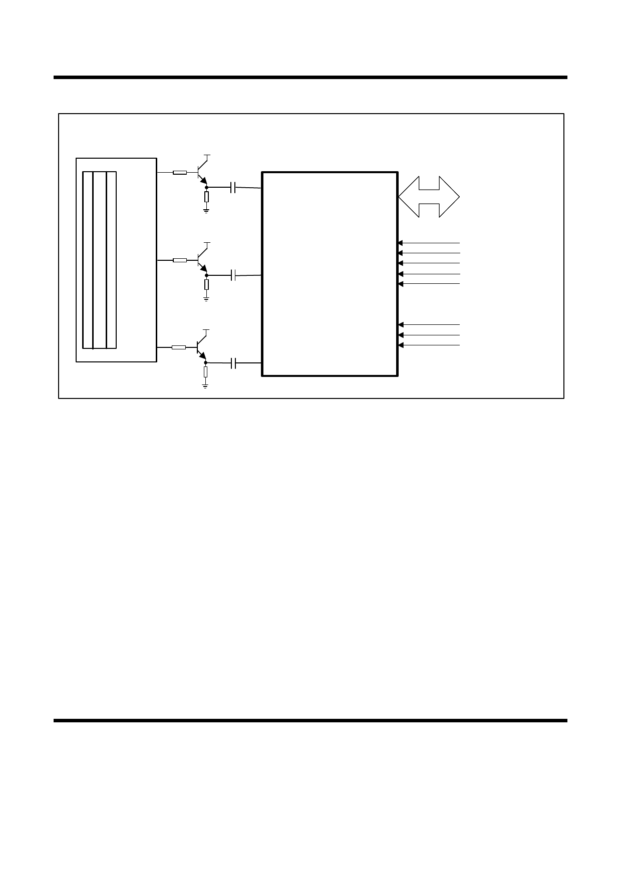
Figure 1 System Diagram
The WM8143-12 signal processing IC interfaces
typically via buffering and AC coupling to the output of
CCD image sensors. The WM8143-12 also interfaces
to CIS image sensors via DC coupling.
Analogue output signals from the image sensor are
sampled, amplified and offset-corrected by the IC
before being converted into digital form by an on-board
high-speed 12-bit resolution analogue to digital
converter. Figure 1 illustrates a typical system
implementation where the three colour outputs from the
CCD image sensor are buffered and AC coupled to the
analogue inputs of the WM8143-12.
The digital interface to the WM8143-12 can be divided
into three distinct sections: -
• Parallel Data I/O
• Digital Control/Serial Timing
• Analogue Interface Timing
These sections are constructed for ease of use by the
system designer and are described in detail on the
following pages of this datasheet.
Wolfson Microelectronics
8
PD. Rev 4 Nov. 99
Share Link: 