X1228 データシートの表示(PDF) - Intersil
部品番号
コンポーネント説明
メーカー
X1228 Datasheet PDF : 29 Pages
| |||
X1228
ABSOLUTE MAXIMUM RATINGS
Temperature Under Bias ................... -65°C to +135°C
Storage Temperature ........................ -65°C to +150°C
Voltage on VCC, VBACK and PHZ/IRQ
pin (respect to ground) ............................-0.5V to 7.0V
Voltage on SCL, SDA, X1 and X2
pin (respect to ground) ............... -0.5V to 7.0V or 0.5V
above VCC or VBACK (whichever is higher)
DC Output Current .............................................. 5 mA
Lead Temperature (Soldering, 10 sec) .............. 300°C
Stresses above those listed under “Absolute Maximum
Ratings” may cause permanent damage to the device.
This is a stress rating only and the functional operation
of the device at these or any other conditions above
those indicated in the operational sections of this
specification is not implied. Exposure to absolute max-
imum rating conditions for extended periods may
affect device reliability.
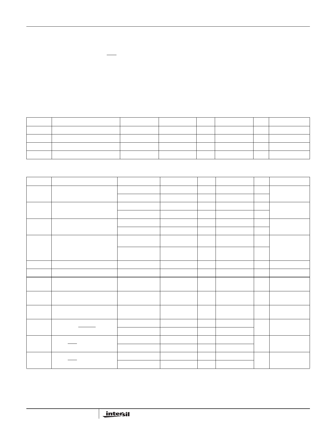
DC OPERATING CHARACTERISTICS (Temperature = -40°C to +85°C, unless otherwise stated.)
Symbol
VCC
VBACK
VCB
VBC
Parameter
Main Power Supply
Backup Power Supply
Switch to Backup Supply
Switch to Main Supply
Conditions
Min
Typ
Max
Unit
2.7
5.5
V
1.8
5.5
V
VBACK -0.2
VBACK
VBACK -0.1
V
VBACK +0.2
V
Notes
OPERATING CHARACTERISTICS
Symbol
Parameter
Conditions
Min
ICC1
ICC2
ICC3
IBACK
Read Active Supply
Current
Program Supply Current
(nonvolatile)
Main Timekeeping
Current
Timekeeping Current –
(Low Voltage Sense and
Watchdog Timer
disabled
VCC = 2.7V
VCC = 5.0V
VCC = 2.7V
VCC = 5.0V
VCC = 2.7V
VCC = 5.0V
VBACK = 1.8V
VBACK = 3.3V
ILI
Input Leakage Current
ILO
Output Leakage Current
VIL
VIH
VHYS
VOL1
VOL2
VOH2
Input LOW Voltage
Input HIGH Voltage
Schmitt Trigger Input
Hysteresis
Output LOW Voltage for
SDA and RESET
Output LOW Voltage for
PHZ/IRQ
Output HIGH Voltage for
PHZ/IRQ
-0.5
VCC related level
VCC = 2.7V
VCC = 5.5V
VCC = 2.7V
VCC = 5.5V
VCC = 2.7V
VCC = 5.5V
VCC x 0.7 or
VBACK x 0.7
.05 x VCC or
.05 x VBACK
VCC x 0.7
VCC x 0.7
Typ
1.25
1.5
Max
400
800
2.5
3.0
10
20
Unit
µA
µA
mA
mA
µA
µA
Notes
1, 5, 7, 14
2, 5, 7, 14
3, 7, 8, 14, 15
µA 3, 6, 9, 14, 15
“See Perfor-
µA mance Data”
10
µA
10
10
µA
10
VCC x 0.2 or
VBACK x 0.2
V
13
VCC + 0.5 or
VBACK + 0.5
V
13
V
13
0.4
V
11
0.4
VCC x 0.3
V
11
VCC x 0.3
V
12
4
FN8100.4
May 18, 2006
Share Link: 