X1228 データシートの表示(PDF) - Intersil
部品番号
コンポーネント説明
メーカー
X1228 Datasheet PDF : 29 Pages
| |||
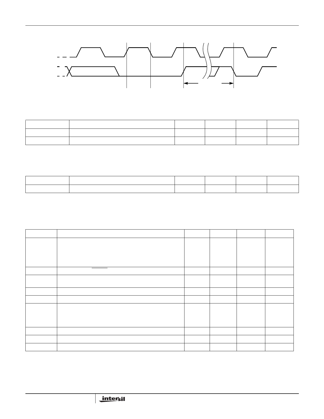
Write Cycle Timing
X1228
SCL
SDA
8th Bit of Last Byte
ACK
tWC
Stop
Condition
Start
Condition
Power-up Timing
Symbol
Parameter
Min.
Typ.(2)
Max.
Units
tPUR(1)
Time from Power-up to Read
1
ms
tPUW(1)
Time from Power-up to Write
5
ms
Notes: (1) Delays are measured from the time VCC is stable until the specified operation can be initiated. These parameters are not 100% tested.
VCC slew rate should be between 0.2mV/µsec and 50mV/µsec.
(2) Typical values are for TA = 25°C and VCC = 5.0V
Nonvolatile Write Cycle Timing
Symbol
Parameter
Min.
Typ.(1)
Max.
Units
tWC(1)
Write Cycle Time
5
10
ms
Note: (1) tWC is the time from a valid stop condition at the end of a write sequence to the end of the self-timed internal nonvolatile write cycle. It is
the minimum cycle time to be allowed for any nonvolatile write by the user, unless Acknowledge Polling is used.
WATCHDOG TIMER/LOW VOLTAGE RESET OPERATING CHARACTERISTICS
Watchdog/Low Voltage Reset Parameters (SeeFigures 3 and 4)
Symbols
Parameters
Min.
Typ.
VPTRIP
tRPD
tPURST
Programmed Reset Trip Voltage
X1228-4.5A
X1228
X1228-2.7A
X1228-2.7
VCC Detect to RESET LOW
Power-up Reset Time-out Delay
4.50
4.63
4.25
4.38
2.75
2.85
2.55
2.65
100
250
tF
VCC Fall Time
10
tR
VCC Rise Time
10
tWDO
Watchdog Timer Period (Crystal = 32.768kHz):
WD1 = 0, WD0 = 0
WD1 = 0, WD0 = 1
WD1 = 1, WD0 = 0
1.7
1.75
725
750
225
250
tRST
Watchdog Reset Time-out Delay (Crystal=32.768kHz)
225
250
tRSP
2-Wire interface
1
VRVALID
Reset Valid VCC
1.0
Max.
4.75
4.50
2.95
2.75
500
400
1.8
775
275
275
Unit
V
ns
ms
µs
µs
s
ms
ms
ms
µs
V
7
FN8100.4
May 18, 2006
Share Link: 