X28C010D データシートの表示(PDF) - Intersil
部品番号
コンポーネント説明
メーカー
X28C010D Datasheet PDF : 23 Pages
| |||
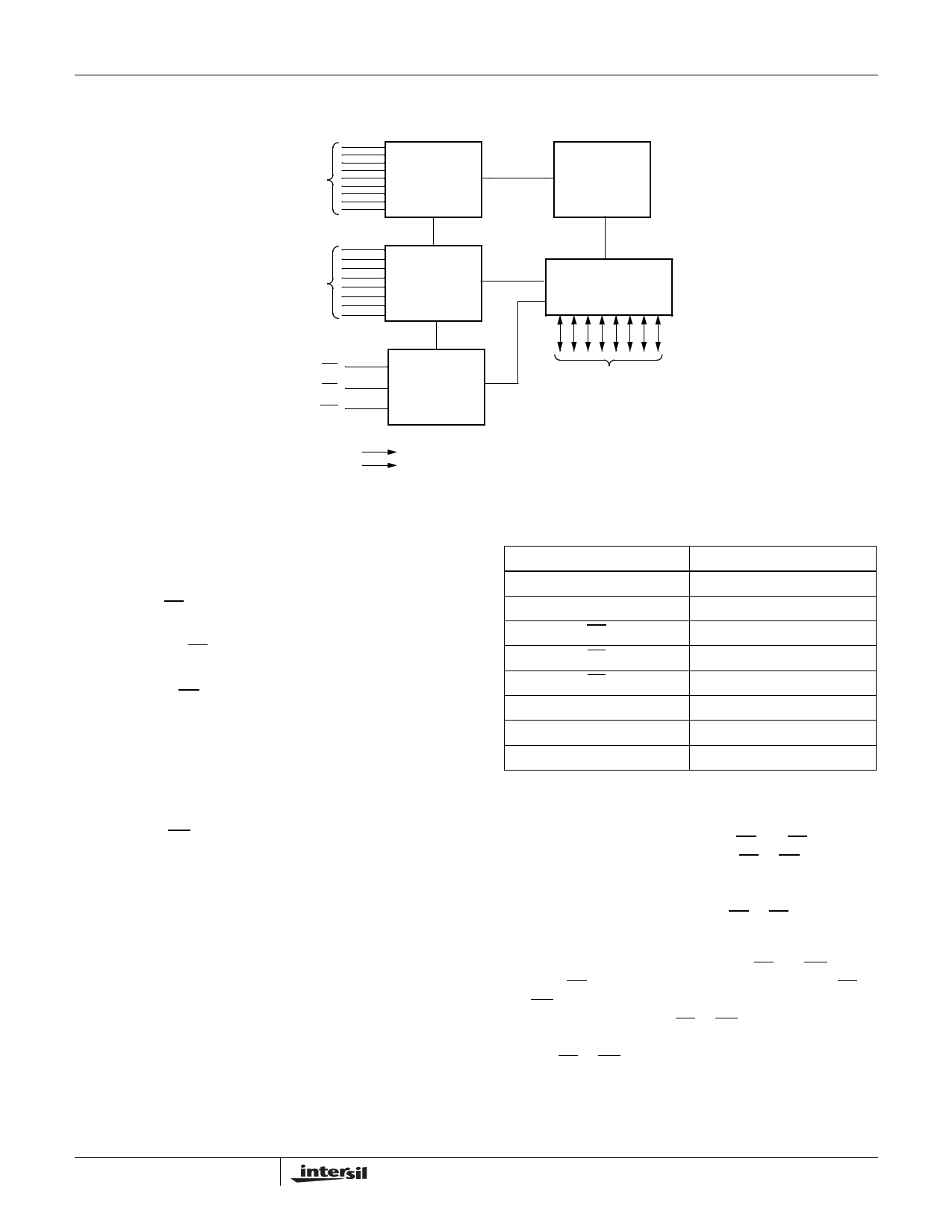
Block Diagram
A8-A16
X28C010
X Buffers
Latches and
Decoder
1Mbit
EEPROM
Array
A0-A7
Y Buffers
Latches and
Decoder
I/O Buffers
and Latches
CE
OE
WE
VCC
VSS
Control
Logic and
Timing
Pin Descriptions
Addresses (A0-A16)
The Address inputs select an 8-bit memory location during a
read or write operation.
Chip Enable (CE)
The Chip Enable input must be LOW to enable all read/write
operations. When CE is HIGH, power consumption is
reduced.
Output Enable (OE)
The Output Enable input controls the data output buffers,
and is used to initiate read operations.
Data In/Data Out (I/O0-I/O7)
Data is written to or read from the X28C010 through the I/O
pins.
Write Enable (WE)
The Write Enable input controls the writing of data to the
X28C010.
I/O0-I/O7
Data Inputs/Outputs
Pin Names
SYMBOL
A0-A16
I/O0-I/O7
WE
CE
OE
VCC
VSS
NC
DESCRIPTION
Address Inputs
Data Input/Output
Write Enable
Chip Enable
Output Enable
+5V
Ground
No Connect
Device Operation
Read
Read operations are initiated by both OE and CE LOW. The
read operation is terminated by either CE or OE returning
HIGH. This two line control architecture eliminates bus
contention in a system environment. The data bus will be in
a high impedance state when either OE or CE is HIGH.
Write
Write operations are initiated when both CE and WE are
LOW and OE is HIGH. The X28C010 supports both a CE
and WE controlled write cycle. That is, the address is latched
by the falling edge of either CE or WE, whichever occurs
last. Similarly, the data is latched internally by the rising edge
of either CE or WE, whichever occurs first. A byte write
operation, once initiated, will automatically continue to
completion, typically within 5ms.
3
FN8105.0
May 11, 2005
Share Link: 