ICX085 データシートの表示(PDF) - Sony Semiconductor
部品番号
コンポーネント説明
メーカー
ICX085
Sony Semiconductor

ICX085 Datasheet PDF : 20 Pages
| |||
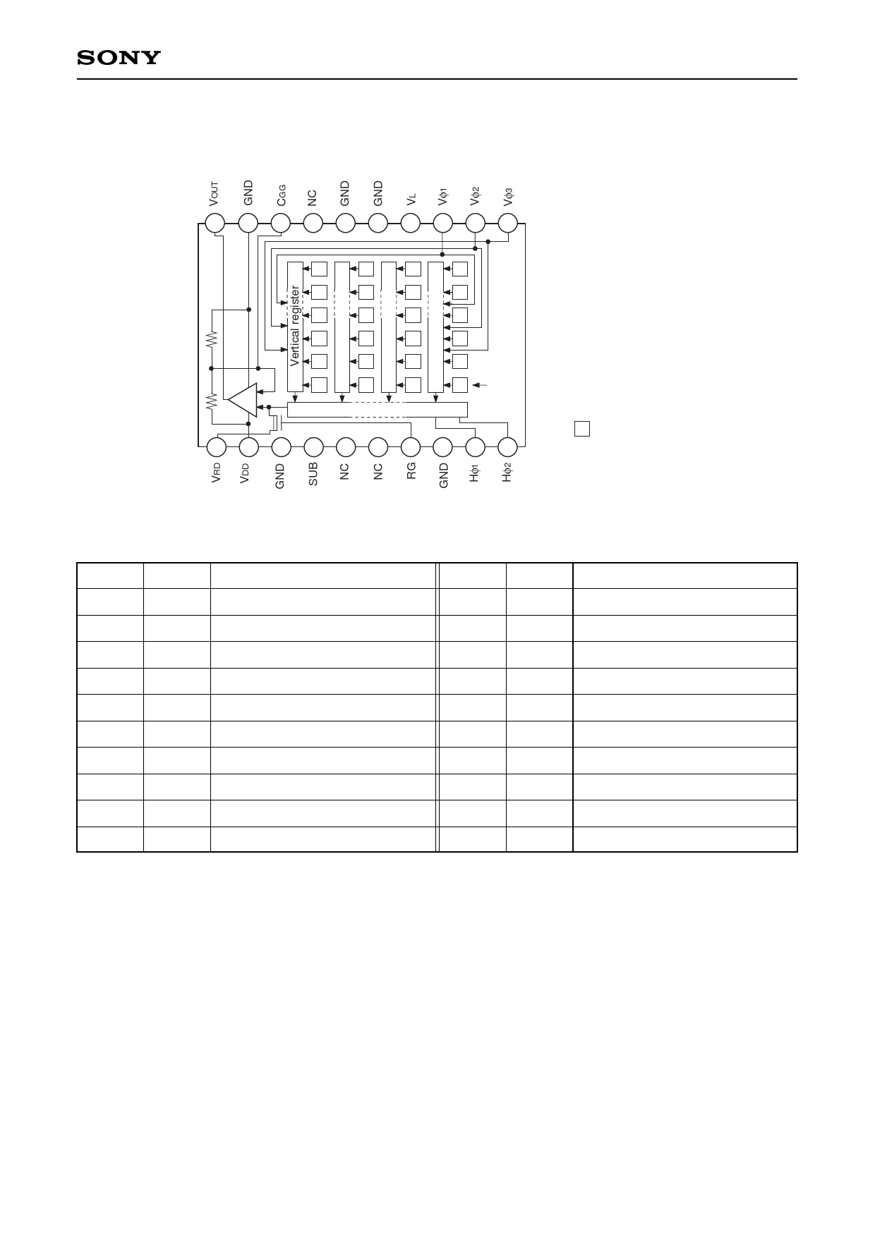
Block Diagram and Pin Configuration
(Top View)
10 9 8 7 6 5 4 3 2 1
ICX085AL
Horizontal register
Note)
11 12 13 14 15 16 17 18 19 20
Note)
: Photo sensor
Pin Description
Pin No. Symbol
Description
Pin No. Symbol
Description
1
Vφ3
Vertical register transfer clock
11
VRD
Reset drain power supply
2
Vφ2
Vertical register transfer clock
12
VDD
Supply voltage
3
Vφ1
Vertical register transfer clock
13 GND GND
4
VL
Protective transistor bias
14 SUB Substrate (overflow drain)
5 GND GND
15 NC
6 GND GND
16 NC
7 NC
8
CGG
Output amplifier gate∗1
17 RG
Reset gate clock
18 GND GND
9 GND GND
19 Hφ1
Horizontal register transfer clock
10
VOUT
Signal output
20 Hφ2
Horizontal register transfer clock
∗1 DC bias is applied within the CCD, so that this pin should be grounded externally through a capacitance of
1µF or more.
–2–
Share Link: