ICX434AQ データシートの表示(PDF) - Sony Semiconductor
部品番号
コンポーネント説明
メーカー
ICX434AQ
Sony Semiconductor

ICX434AQ Datasheet PDF : 23 Pages
| |||
ICX434AQ
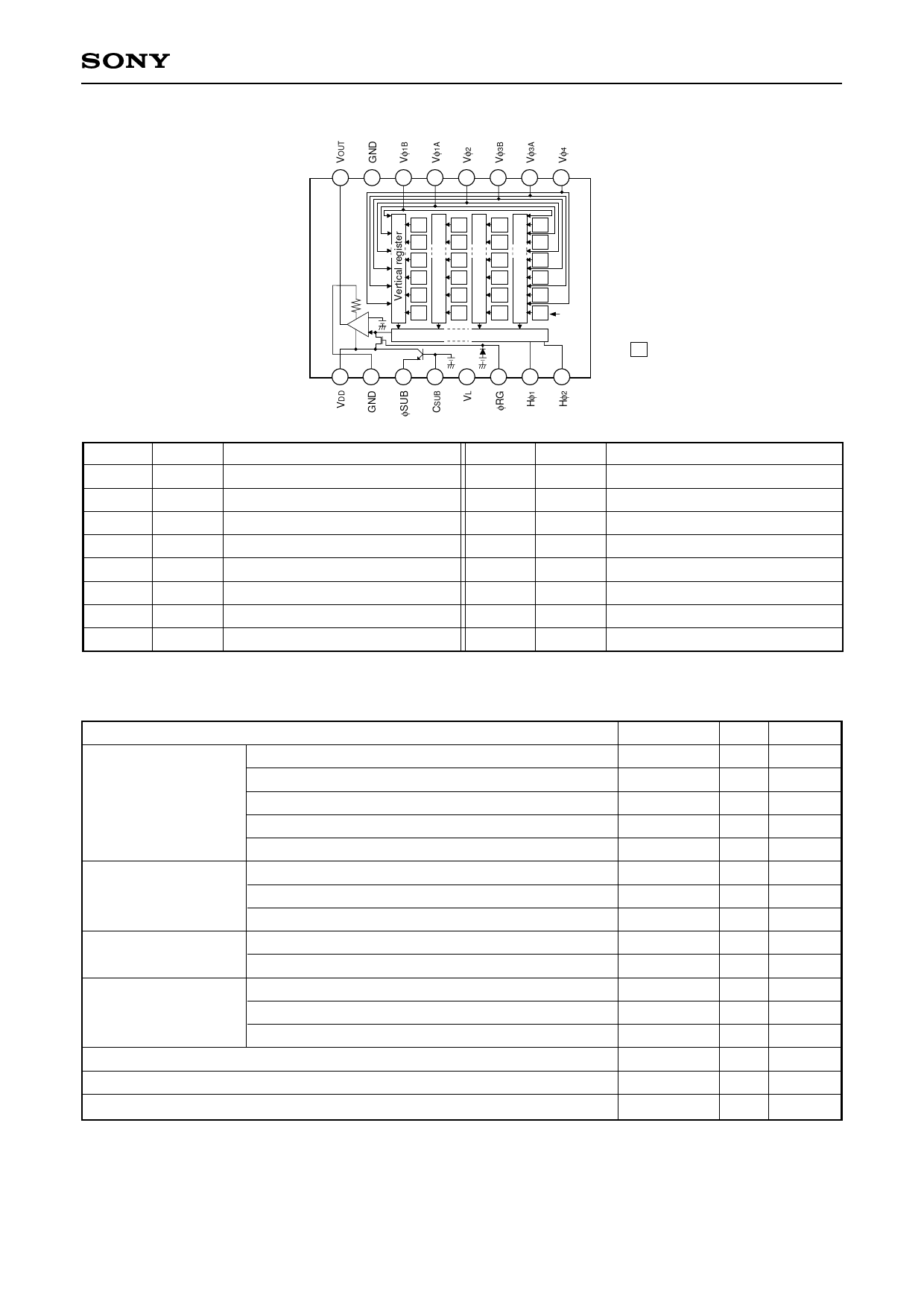
Block Diagram and Pin Configuration
(Top View)
8
7
6
5
4
3
2
1
G
B
G
R
G
R
G
B
G
R
G
R
G
B
G
R
G
R
Horizontal register
B
G
B
G
B
G Note)
Note) : Photo sensor
9 10 11 12 13 14 15 16
Pin Description
Pin No. Symbol
Description
Pin No. Symbol
Description
1
Vφ4
Vertical register transfer clock
9
VDD
Supply voltage
2
Vφ3A
Vertical register transfer clock
10 GND GND
3
Vφ3B
Vertical register transfer clock
4
Vφ2
Vertical register transfer clock
11 φSUB Substrate clock
12
CSUB
Substrate bias∗1
5
Vφ1A
Vertical register transfer clock
13 VL
Protective transistor bias
6
Vφ1B
Vertical register transfer clock
14 φRG
Reset gate clock
7 GND GND
15 Hφ1
Horizontal register transfer clock
8
VOUT
Signal output
16 Hφ2
Horizontal register transfer clock
∗1 DC bias is generated within the CCD, so that this pin should be grounded externally through a capacitance
of 0.1µF.
Absolute Maximum Ratings
Against φSUB
Against GND
Against VL
Between input clock
pins
Storage temperature
Item
VDD, VOUT, φRG – φSUB
Vφ1A, Vφ1B, Vφ3A, Vφ3B – φSUB
Vφ2, Vφ4, VL – φSUB
Hφ1, Hφ2, GND – φSUB
CSUB – φSUB
VDD, VOUT, φRG, CSUB – GND
Vφ1A, Vφ1B, Vφ2, Vφ3A, Vφ3B, Vφ4 – GND
Hφ1, Hφ2 – GND
Vφ1A, Vφ1B, Vφ3A, Vφ3B – VL
Vφ2, Vφ4, Hφ1, Hφ2, GND – VL
Voltage difference between vertical clock input pins
Hφ1 – Hφ2
Hφ1, Hφ2 – Vφ4
Ratings
–40 to +12
–50 to +15
–50 to +0.3
–40 to +0.3
–25 to
–0.3 to +22
–10 to +18
–10 to +6.5
–0.3 to +28
–0.3 to +15
to +15
–6.5 to +6.5
–10to +16
–30 to +80
Unit Remarks
V
V
V
V
V
V
V
V
V
V
V
∗2
V
V
°C
Guaranteed temperature of performance
–10 to +60 °C
Operating temperature
–10 to +75 °C
∗2 +24V (Max.) when clock width < 10µs, clock duty factor < 0.1%.
+16V (Max.) is guaranteed for turning on or off power supply.
–2–
Share Link: