XC62ER5001MR データシートの表示(PDF) - TOREX SEMICONDUCTOR
部品番号
コンポーネント説明
メーカー
XC62ER5001MR Datasheet PDF : 12 Pages
| |||
XC62E
Series
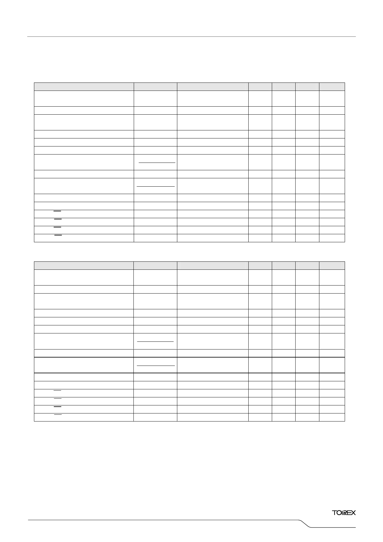
■ELECTRICAL CHARACTERISTICS (Continued)
XC62EP4002
VOUT(T)=4.0V(*1)
PARAMETER
SYMBOL
Output Voltage
VOUT(E) (*2)
Maximum Output Current (*6)
Load Regulation (*6)
IOUT max
△VOUT
Dropout Voltage (*3)
Supply Current 1
Supply Current 2
Line Regulation (*6)
Input Voltage
Output Voltage
Temperature Characteristics (*6)
EXT Output Voltage
EXT Leak Current
CE "High" Level Voltage
CE "Low" Level Voltage
CE "High" Level Current
CE "Low" Level Current
Vdif
ISS1
ISS2
△VOUT
△VIN・VOUT
VIN
△VOUT
△Topr・VOUT
VEXT
ILEAK
VCEH
VCEL
ICEH
ICEL
CONDITIONS
IOUT=50mA
VIN=5.0V
VIN=5.0V
VIN=5.0V
1mA≦IOUT≦100mA
IOUT=100mA
VIN=5.0V, VCE=VSS
VIN=8.0V,VCE=VIN
IOUT=50mA
5.0V≦VIN≦8.0V
IOUT=10mA
-30℃≦Topr≦80℃
VCE=VIN
VCE=VSS
MIN.
3.920
-
-60
-
-
-
-
-
-
-
-
1.5
-
-
-0.2
TYP.
4.000
1000
-
100
50
-
0.1
-
±100
-
-
-
-
-
-0.05
MAX.
4.080
-
60
-
80
0.6
0.3
8.0
-
8.0
0.5
-
0.25
0.1
0
Ta=25℃
UNITS
V
mA
mV
mV
μA
μA
%V
V
ppm/℃
V
μA
V
V
μA
μA
XC62EP4002
VOUT(T)=5.0V(*1)
PARAMETER
Output Voltage
Maximum Output Current (*6)
Load Regulation (*6)
Dropout Voltage (*3)
Supply Current 1
Supply Current 2
Line Regulation (*6)
Input Voltage
Output Voltage
Temperature Characteristics (*6)
EXT Output Voltage
EXT Leak Current
CE "High" Level Voltage
CE "Low" Level Voltage
CE "High" Level Current
CE "Low" Level Current
SYMBOL
VOUT(E) (*2)
IOUT max
△VOUT
Vdif
ISS1
ISS2
△VOUT
△VIN・VOUT
VIN
△VOUT
△Topr・VOUT
VEXT
ILEAK
VCEH
VCEL
ICEH
ICEL
CONDITIONS
IOUT=50mA
VIN=6.0V
VIN=6.0V
VIN=6.0V
1mA≦IOUT≦100mA
IOUT=100mA
VIN=6.0V, VCE=VSS
VIN=8.0V,VCE=VIN
IOUT=50mA
6.0V≦VIN≦8.0V
IOUT=10mA
-30℃≦Topr≦80℃
VCE=VIN
VCE=VSS
MIN.
4.940
-
-60
-
-
-
-
-
-
-
-
1.5
-
-
-0.2
TYP.
5.000
1000
-
100
50
-
0.1
-
±100
-
-
-
-
-
-0.05
MAX.
5.100
-
60
-
80
0.6
0.3
8.0
-
8.0
0.5
-
0.25
0.1
0
The characteristics for the XC62ER series are the same as above except for the CE operating logic, which is the opposite.
Ta=25℃
UNITS
V
mA
mV
mV
μA
μA
%V
V
ppm/℃
V
μA
V
V
μA
μA
Note: *1. VOUT(T)=Specified output voltage.
*2. VOUT(E)=Effective output voltage (i.e. the output voltage when "VOUT(T)+1.0V" is provided at the VIN pin while maintaining a
certain IOUT value).
*3. Vdif= {VIN1 (*5)-VOUT1 (*4)}
*4. VOUT1= A voltage equal to 98% of the output voltage whenever an amply stabilized IOUT {VOUT(T)+1.0V} is input.
*5. VIN1= The input voltage when VOUT1 appears as input voltage is gradually decreased.
*6. The characteristics for the parameters are liable to vary depending on which transistor is used.
Please use a transistor with a low saturation voltage level and hFE equal to 100 or more.
*7. The maximum output current value is not a value representing continuous output due to the limitations of the 2AS1213
transistor's power dissipation.
5/12
Share Link: 