XC6229 データシートの表示(PDF) - TOREX SEMICONDUCTOR
部品番号
コンポーネント説明
メーカー
XC6229
TOREX SEMICONDUCTOR

XC6229 Datasheet PDF : 26 Pages
| |||
XC6229 Series
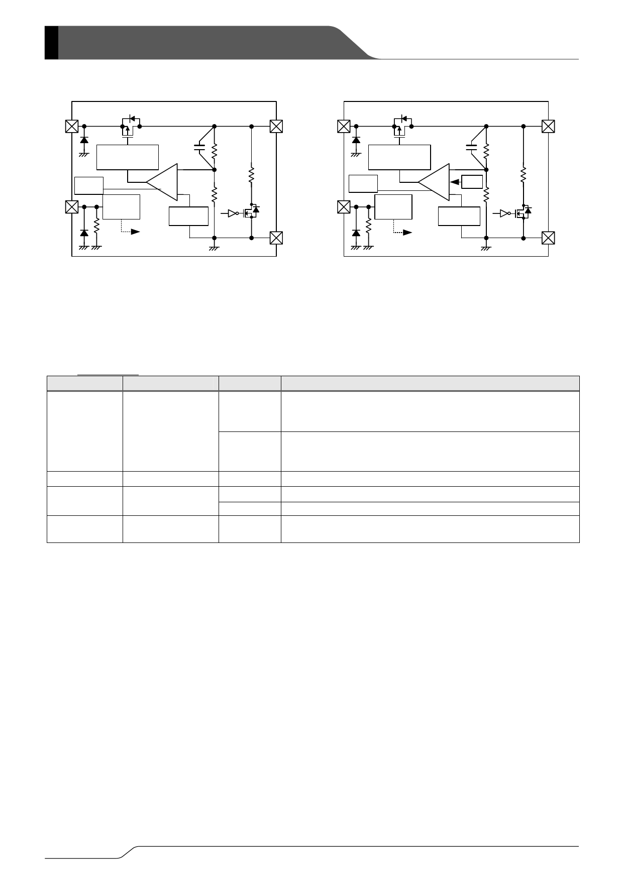
■BLOCK DIAGRAMS
VIN
VOUT VIN
VOUT
CurrentLimit
CFB
R1
CurrentLimit
CFB
R1
Error+
Rdischg
TSD
Amp-
R2
CE
ON/OFF
Control
Voltage
Reference CE
Error+
Non
Rdischg
TSD
Amp
Rush
-
R2
CE
ON/OFF
Control
Voltage
Reference CE
each
each
VSS
circuit
VSS
circuit
XC6229series Type D
* Diodes inside the circuits are ESD protection diodes and parasitic diodes.
XC6229series Type H
■PRODUCT CLASSIFICATION
●Ordering Information
XC6229①②③④⑤⑥-⑦(*1)
DESIGNATOR
ITEM
①
Type of Regulator
②③
④
⑤⑥-⑦(*1)
Output Voltage
Output Voltage
(2nd decimal place)
Package
(Order Unit)
SYMBOL
D
H
12〜40
1
B
1R-G
DESCRIPTION
CE Active High
Without Inrush Current Protection
With CE Pull-down, With CL discharge
CE Active High
With Inrush Current Protection
With CE Pull-down, With CL discharge
ex.) 2.80V → ②=2, ③=8, ④=please see down below.
±1%, In case of 2nd decimal place 0 (ex.2.80V → ④=1)
±1%, In case of 2nd decimal place 5 (ex.2.85V → ④=B)
LGA-4B01 (5,000 /Reel)
(*1) The “-G” suffix denotes Halogen and Antimony free as well as being fully EU RoHS compliant.
2/26
Share Link: