LR38603 データシートの表示(PDF) - Sharp Electronics
部品番号
コンポーネント説明
メーカー
LR38603 Datasheet PDF : 26 Pages
| |||
LR38603
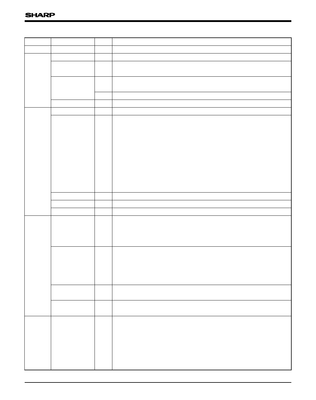
DSP REGISTER TABLE
ADDRESS
NAME
BIT
CONTENTS
00h STOP_EEPROM [7 : 0] Stop reading from EEPROM only when EEPROM data is FF.
01h LPF_TH
[7] H : Luminance signal processing without LPF (when using B/W CCD)
CCD_SEL
[6 : 5] 00 : 270 k pixel CCD (NTSC) 01 : 410 k pixel CCD (NTSC)
10 : 320 k pixel CCD (PAL) 11 : 470 k pixel CCD (PAL)
ADTI
[4 : 3] Input data timing adjustment
00 : Reference 01 : 1 clock delay 10 : 1 clock forward 11 : 2 clocks forward
[2] 1 : Latch with inverted clock
SEL_CDS
[1 : 0] Fixed to 1X (IR3Y48A1)
02h NI
[6] 0 : Interlace 1 : Non-interlace
MODE_OUT_SIG
Select output mode.
[5 : 3]
000 : Analog video output
EXCKI : Vertical reset pulse input
001 : Analog video output EXCKI : 8 fsc clock input
EEMD2 : Horizontal reset pulse input EEMD3 : Vertical reset pulse input
010 : Analog video output EEMD2 : Horizontal reset pulse input
EEMD3 : Vertical reset pulse input
100 : YUV digital video output : Clock rate of video data pixel-CK
101 : YUV digital video output : Clock rate of video data EXCKI
110 : UYVY digital video output : Clock rate of video data EXCKI
011, 111 are prohibited.
START_EE
[2] Shutter speed at power-on 0 : minimum 1 : maximum
AGC_FIX
[1] PGA control
0 : Auto
1 : Fixed
OB_SEL
[0] Carrier balance control
0 : Auto
1 : Fixed
03h HD_SEL
[6 : 5] Select output signal from HD pin
00 : HD output (CCD drive timing) 01 : HD output (video output timing)
10 : BELL pulse (in analog video output), HREF (in digital video output)
11 : Fixed to L level
VD_SEL
[4 : 3] Select output signal from VD pin
00 : VD output (CCD drive timing) 01 : VD output (video output timing)
10 : Fixed to L level (in analog video output), VS (in digital video output)
11 : Fixed to L level (in analog video output), CSYNC (in digital video
output)
DCK1_SEL
[2 : 1] Select output signal from DCK1 pin (in analog video output)
00 : CSYNC 01 : CBLNK 1X : Fixed to L level
DCK2_SEL
[0] Select output signal from DCK2 pin (in analog video output)
0 : Fluorescent signal 1 : Fixed to L level
04h SW_CTRL
[7 : 0] Electronic shutter control (EEMDS, EEMD1, EEME2, EEMD3), mirror video
output (MIR [MSB]), internal register for exposure-standard (BLC) and white
balance (WB2, WB1 [LSB]) are set when selecting digital output mode with
MODE_OUT_SIG (address 02h).
Shutter control of EEMD2 and EEMD3 is set by the register of SW_CTRL
and that of EEMDS and EEMD1 is set by pin 41 and pin 42 when setting
"001" and "010" with MODE_OUT_SIG (address 02h).
7
Share Link: 