LC83026E データシートの表示(PDF) - SANYO -> Panasonic
部品番号
コンポーネント説明
メーカー
LC83026E Datasheet PDF : 16 Pages
| |||
LC83026E
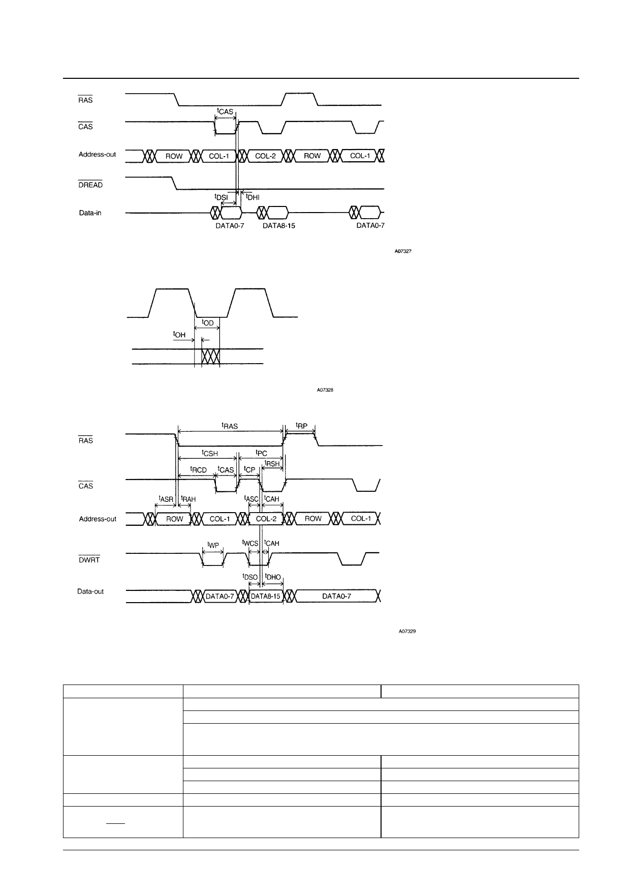
(A0 to A8)
(D0 to D3)
Figure 6 External DRAM Data Input Timing
Transfer bit clock
(BCKO)
Output data
(ASO)
Figure 7 Audio Data Output Timing
(A0 to A8)
(D0 to D3)
Figure 8 External DRAM Data Output Timing
Differences between the LC83025E and the LC83026E
Parameter
LC83025E
LC83026E
Decimation filter improved
A/D converter block
Input comparator improved
*: The VREF pin was added in association with the improvements to the input comparator. The VREF pin external
capacitor must be located as close as possible to the LC83026E, and must be connected with lines that are as
short as possible.
4 × oversampling filters used
2 × oversampling filters used
D/A converter block
Second-order noise shaping
Third-order noise shaping
Single-pin output used.
Two-pin output operation
Reset time
One or more sampling period
Two or more sampling periods
When no digital input is provided The LRCKI and BCKI pins must be connected to the
(when the SELC pin is low)
LRCKO and BCKO pins.
The LRCKI and BCKI pins must be connected to either
VDD or VSS; they do not need to be connected to the
LRCKO and BCKO pins.
No. 5663-9/16
Share Link: 