NJU8402D データシートの表示(PDF) - Japan Radio Corporation
部品番号
コンポーネント説明
メーカー
NJU8402D Datasheet PDF : 10 Pages
| |||
NJU8402
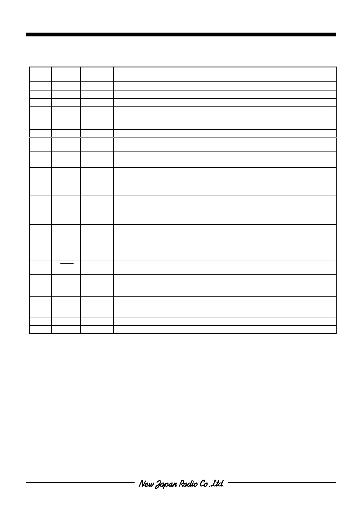
s TERMINAL DESCRIPTION
PIN
No.
SYMBOL
INPUT
/OUTPUT
FUNCTION
1
VDD
16
VSS
8
AVDD
9
AVSS
2
MCKI
Digital Power Supply, +5V
Digital GND, 0V
Analog Power Supply, +5V
Analog GND, 0V
I
Master Clock Input Terminal
The input signal frequency is 256 times or 384 times of fs.
13
DIN
I
Serial Audio Data Input Terminal
14 LRCK
I
L/R Channel Clock Input Terminal
This clock must synchronize with MCKI.
15 BCLK
I
Audio Serial Data Clock Input Terminal
This clock must synchronize with MCKI.
3
SCK
Control Register Serial Data Sift Clock Input Terminal
I
Control register leads the control data synchronizing the rising edge of SCK
signal. When the control register is not used, the state of SCK terminal has to
keep level ”H”.
4
DATA
Control Register Serial Data Input Terminal
I
Input data sets various functions.
When the control register is not used, the state of DATA terminal has to keep level
“H”.
5
REQ
Control Register Serial Data Request Input Terminal
The control data are latched in the control register at the rising edge of REQ
I
signal.
When the control register is not used, the state of REQ terminal has to keep level
“H”.
12
RST
I
Reset
“L” level signal into reset terminal initializes the system.
7 VCOML
Left channel Analog Signal Common Terminal for Connecting Smooth Capacitor
A chemical capacitor should be connected between this terminal and AVSS for
stabilizing.
10 VCOMR
Right Channel Analog Signal Common Terminal for Connecting Smooth Capacitor
A chemical capacitor should be connected between this terminal and AVSS for
stabilizing.
6 AOUTL
O
L-Channel Analog Signal Output Terminal
11 AOUTR
O
R-Channel Analog Signal Output Terminal
-2-
Share Link: 