HSP50215 データシートの表示(PDF) - Intersil
部品番号
コンポーネント説明
メーカー
HSP50215 Datasheet PDF : 21 Pages
| |||
HSP50215
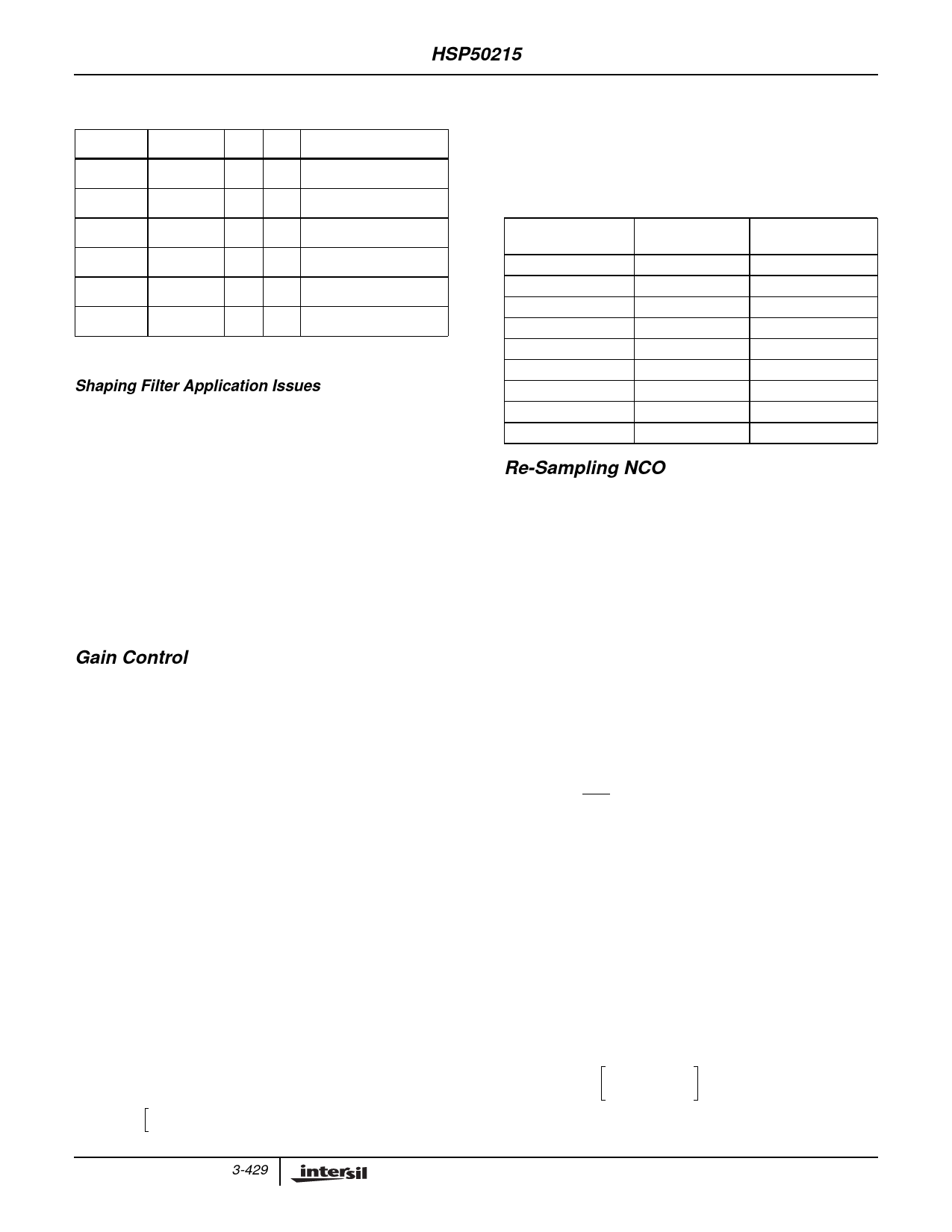
TABLE 2. EXAMPLES OF THE DIFFERENT CASES AND
DIFFERENT FIR INPUT SAMPLING FREQUENCIES
EXAMPLE
fCLK
DS IP
MAX fS
1
52MHz 16 16 52/256 = 203kHz
2
52MHz 16 8 52/128 = 406kHz
3
52MHz 16 4 52/64 = 813kHz
4
52MHz 10 4 52/40 = 1300kHz
5
52MHz
8 4 52/32 = 1625kHz
6
52MHz
4 4 52/16 = 3,250kHz
(fCLK = 48MHz for industrial temperature range).
Shaping Filter Application Issues
Note that when using quadrature modulation,
saturation/overflow can occur when the input values for I and Q
exceed 0.707 peak. Also note that there is gain in Interpolation
filter. Because of these two implementation constraints, the
Shaping filter coefficients may need to be reduced from full
scale to provide unity gain in the PUC and to prevent saturation
in the shaping filter. After the shaping filter computation, a gain
scaling control is provided. It is possible to allow the shaping
filter computation to approach unity on each channel and then
scale the I/Q magnitudes in the Gain Control.
The delay through the shaping and interpolation filters is 20
CLKs and the shaping filter delay.
Gain Control
Between the Shaping filter and the Interpolation filter is a gain
adjustment stage that provides for identical scaling of the I
and Q shaped signals. Gain adjustment is from 0 to slightly
less than unity. This gain control can be used to prevent signal
overflow in the Interpolation filter or saturation in the
quadrature mixer.
The interpolation filter can have a gain of 2dB. If a full scale
signal is required at the output of the shaping filter, apply 2dB
back off in the Gain Adjust Circuit. For worst case conditions,
the interpolation filter can have 25% overshoot. (See the
annotations on the Functional Block Diagram). Gain control
can also be used to set the level of a signal prior to summing
multiple signals in the Modulated Output Section.
The scaling multiplier value is programmed using an bits 0-7
in Control Word 17. The attenuation is set by:
Gain = OutGain/28
(EQ. 5)
GaindB = 20log [OutGain ⁄ 28 ]
OutGain = [(Gain)28 ]Hex
OutGain =
(Ga
10
i
ndB
⁄
20
)
28
]H
e
x
(EQ. 5A)
(EQ. 5B)
(EQ. 5C)
where Gain is the desired signal level relative to fullscale,
GaindB is the desired signal level in dB relative to fullscale,
and OutGain is the control word value.
Table 3 details a few key control words and the associated
attenuations for the I and Q signals.
TABLE 3. SCALING GAIN ATTENUATION
CONTROL WORD
1111 1111yt
GAIN
(dBFS)
-0.033996
SCALING GAIN
(VOUT/VIN)%
99.6
1000 0000
-6.021
50.0
0100 0000
-12.041
25.0
0010 0000
-18.062
12.5
0001 0000
-24.082
6.25
0000 1000
-30.103
3.125
0000 0100
-36.124
1.5625
0000 0010
-42.144
0.78125
0000 0001
-48.165
0.390625
Re-Sampling NCO
The Sample Rate NCO provides the sample clock and
sample clock phase information to both the shaping and
Interpolation filters. Figure 8 details the conceptual design.
The sample frequency is set with 30-bit resolution. The LSB is
REFCLK/232. The internal accumulator resolution in 32 bits.
The MSB of the accumulator is the sample clock for the filters.
Four bits of coarse timing phase resolution control the
Shaping filter, while twelve bits of fine timing phase resolution
control the Interpolation filter.
The Resampling NCO frequency control word is double
buffered. The 30-bit timing NCO frequency is written to
Control Addresses 2 and 3. The frequency control word is
transferred from the buffer into the Re-Sampling NCO on a
pulse from SYNCIN or on a write to Control Word 2. Control
Word 22, bit 0, sets which action, (the SYNCIN or write to
CW2), causes a frequency control word transfer in the NCO.
Assertion of RST stops the Re-Sampling NCO and clears
the accumulator contents. It is held disabled until a SYNCIN
or write to Control Word 3 generates an EnNCO signal to
restart the NCO.
The PUC input sample rate is set by the Re-Sampling NCO.
The maximum error is 52MHz/(232) = 0.012Hz for the
commercial part and 48MHz/(232) = 0.011Hz for the
industrial part. The frequency control word is computed by:
FRESAMP = SR(29:0) × fCLK × 2–32
(EQ. 6)
where SR(29:0) is the 30-bit frequency control word and
fCLK is REFCLK.
Equation 6 can be rearranged to solve for SR(29:0).
SR(29:0) = RND -f-R-----Ef--C--S--L-A---K-M-----P-- × 232
The range of SR(29:0) is: [0 to 230 – 1]
3-429
Share Link: 