XE1203F データシートの表示(PDF) - Semtech Corporation
部品番号
コンポーネント説明
メーカー
XE1203F Datasheet PDF : 36 Pages
| |||
XE1203F
RTParam_Bitsync and RTParam_Barker Configuration Register bits are set low (disabled). In this case the
demodulator output is directly connected to the DATA pin and the DCLK pin is set to low. Otherwise, the
demodulator output is processed by the bit synchronizer.
For correct operation of the demodulator the modulation index β of the input signal should meet the following
condition:
β
=
2⋅∆f
BR
≥ 2,
where ∆f is the frequency deviation and BR the bit rate.
4.1.4 Bit synchronizer
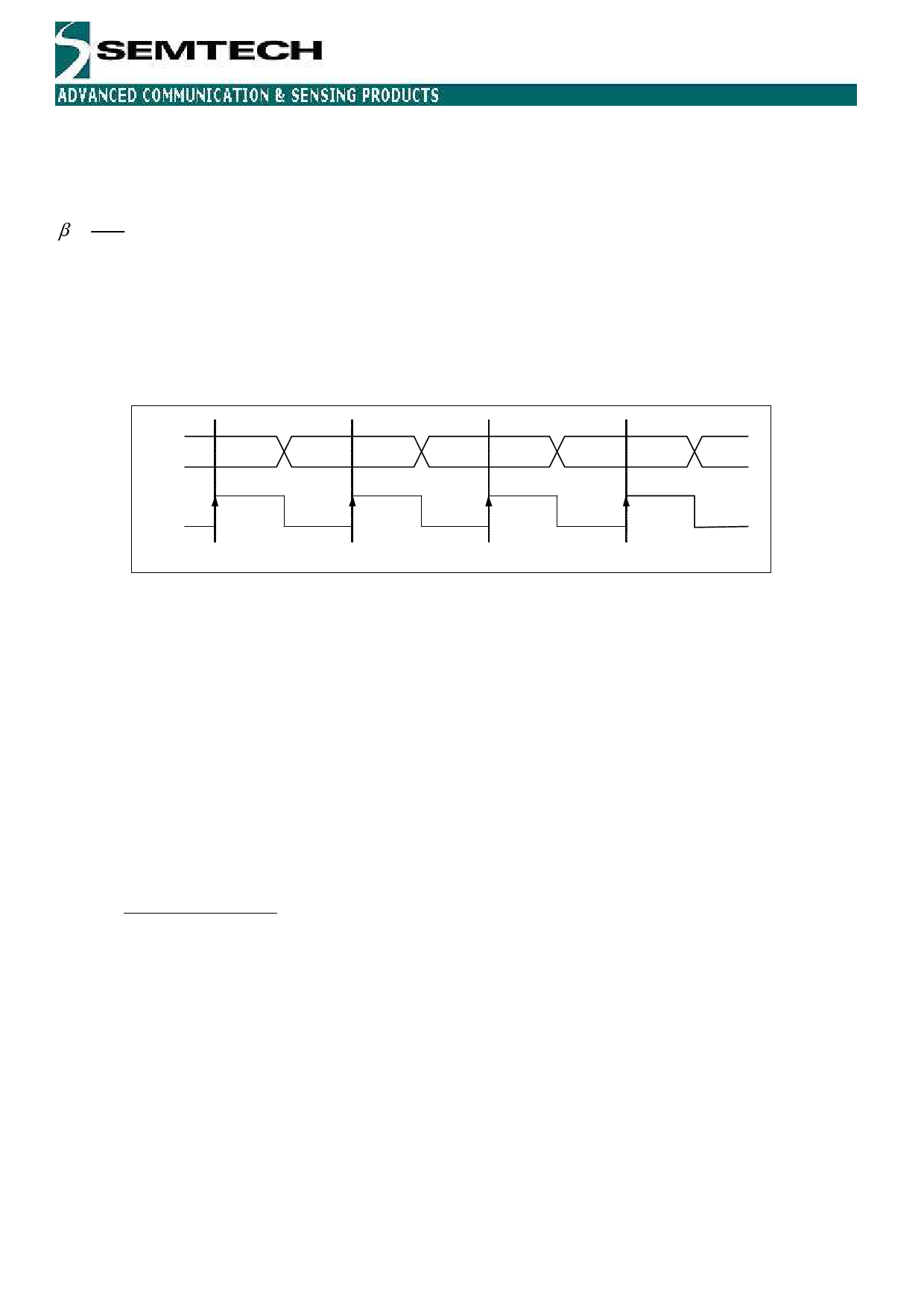
The raw output signal from the demodulator usually contains jitter and glitches. The bit synchronizer transforms the
data output of the demodulator into a glitch-free bit stream available on the DATA pin and generates a synchronized
clock DCLK to be used for sampling the DATA output (see Figure 3, below).
DATA
(NRZ)
DCLK
Figure 3: Bit synchronizer timing diagram.
To ensure the correct operation of the bit synchronizer, in addition to the requirement for the modulation index
defined in 4.1.3 above, the following conditions have to be satisfied:
• A preamble of 24 bits is required for the synchronization,
• The preamble must be a sequence of “0” and “1” sent alternatively,
• During transmission of data, the bit stream must have at least one transition from “0” to “1” or from “1” to “0”
every 8 bits.
• The accuracy of the bit rate must be better than ± 5%.
The bit synchronizer is enabled when RTParam_Bsync Configuration Register bit is high. If this bit set low, the bit
synchronizer is disabled. In this case the output of the demodulator is directed to the DATA pin and the DCLK
output is set to “0”.
The received bit rate is defined by the value of the FSParam_BR Configuration Register, and is calculated as
follows:
Bit rate =
152.34e3
int(FSParam_BR(6 : 0)) + 1
where int(x) is the integer value of the unsigned binary representation of (x).
Note: for Konnex standard operations, the bit rate is fixed at 32.7 kbit/s. ADParam_enable_konnex should be set to
a ‘1’.
4.1.5 The DATA and DATAIN pins
The pin DATA is by default used by both the transmitter and the receiver sections. By default it is set as a
bidirectional I/O pin. When in receive mode, demodulated data appears at DATA as an output signal. In transmit
mode, the transmitted bit stream is applied to this pin as an input.
Some applications may require separate input and output pins for the transmitted and received data. In this case
the user has to set the ADParam_disable_data_bidir Configuration Register bit to ‘1’. As a result the DATA pin is set
as an output only for the received data, while the transmit data is controlled via the DATAIN input pin.
© Semtech 2007
www.semtech.com
9
Share Link: 