RF2484 データシートの表示(PDF) - RF Micro Devices
部品番号
コンポーネント説明
メーカー
RF2484 Datasheet PDF : 10 Pages
| |||
RF2484
Preliminary
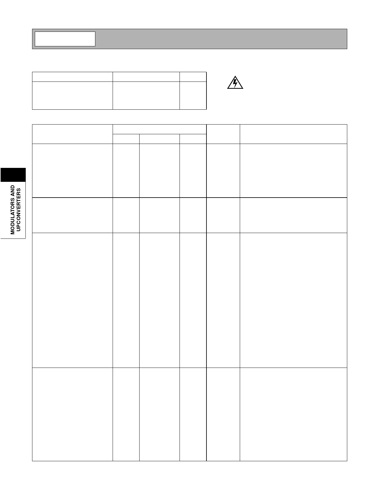
Absolute Maximum Ratings
Parameter
Supply Voltage
Input LO and RF Levels
Operating Ambient Temperature
Storage Temperature
Rating
-0.5 to +7.5
+10
-40 to +85
-40 to +150
Unit
VDC
dBm
°C
°C
Caution! ESD sensitive device.
RF Micro Devices believes the furnished information is correct and accurate
at the time of this printing. However, RF Micro Devices reserves the right to
make changes to its products without notice. RF Micro Devices does not
assume responsibility for the use of the described product(s).
Parameter
LO Input
Frequency Range
Power Level
5
Input Impedance
Modulation Input
Frequency Range
Reference Voltage (VREF)
Input Resistance
Input Bias Current
RF Output (880MHz)
CDMA Output Channel Power
CDMA ACPR
Carrier Suppression
Carrier Suppression
over Temperature
Sideband Suppression
Sideband Suppression
over Temperature
Broadband Noise Floor
EVM
Phase Error
Rho
Output Impedance
RF Output (1960MHz)
PCS CDMA Output Power
PCS CDMA ACPR
Carrier Suppression
Carrier Suppression
over Temperature
Sideband Suppression
Sideband Suppression
over Temperature
5-30
Specification
Min.
Typ.
Max.
800
2500
-6
+6
45 - j95
52 - j54
58 - j50
63 - j40
DC
250
4.1
30
40
-12
-72
50
35
50
35
-152.5
2.3
1
.9993
28 - j72
-13
-72
50
35
50
35
Unit
MHz
dBm
Ω
Ω
Ω
Ω
Condition
T=25°C, VCC=5V, VREF=4.1V; I and Q
driven single-ended
At 880MHz
At 1960MHz
At 2140MHz
At 2400MHz
MHz
V
kΩ
µA
dBm
dBc
dBc
dBc
dBc
dBc
dBm/Hz
%
° RMS
Ω
dBm
dBc
dBc
dBc
dBc
dBc
LO= -5dBm at 880MHz; Single sideband
testing unless otherwise noted
For ACPR =-72dBc; I&Q Amplitude=1.1VPP
(single-ended)
Channel Power=-12dBm; see Test Setup for
detailed information
T=25°C; POUT=-10dBm; optimized I,Q DC
offsets
Temperature cycled from -40°C to +85°C
after optimization at T=25°C; POUT=-10dBm
T=25°C; POUT=-10dBm; optimized I,Q
amplitude and phase balance
Temperature cycled from -40°C to +85°C
after optimization at T=25°C; POUT=-10dBm
At 20MHz offset, 30kHz res BW, VCC=5V;
ISIG, QSIG, IREF, and QREF tied to VREF
See Test Setup for detailed information
See Test Setup for detailed information
See Test Setup for detailed information
LO=-5dBm at 1960MHz; Single sideband
testing unless otherwise noted
For ACPR =-72dBc; I&Q Amplitude=1.2VPP
(single-ended)
Channel Power=-13dBm; see Test Setup for
detailed information
T=25°C; POUT=-13dBm; optimized I,Q DC
offsets
Temperature cycled from -40°C to +85°C
after optimization at T=25°C; POUT=-13dBm
T=25°C; POUT=-13dBm; optimized I,Q
amplitude and phase balance
Temperature cycled from -40°C to +85°C
after optimization at T=25°C; POUT=-13dBm
Rev A2 010829
Share Link: 