XM28C020 データシートの表示(PDF) - Xicor -> Intersil
部品番号
コンポーネント説明
メーカー
XM28C020 Datasheet PDF : 16 Pages
| |||
XM28C020
PIN DESCRIPTIONS
Addresses (A0–A17)
The Address inputs select an 8-bit memory location
during a read or write operation.
Chip Enable (CE)
The Chip Enable input must be LOW to enable all read/
write operations. When CE is HIGH, power consumption
is reduced (see Note 4).
Output Enable (OE)
The Output Enable input controls the data output buffers
and is used to initiate read operations.
Data In/Data Out (I/O0–I/O7)
Data is written to or read from the XM28C020 through
the I/O pins.
Write Enable (WE)
The Write Enable input controls the writing of data to the
XM28C020.
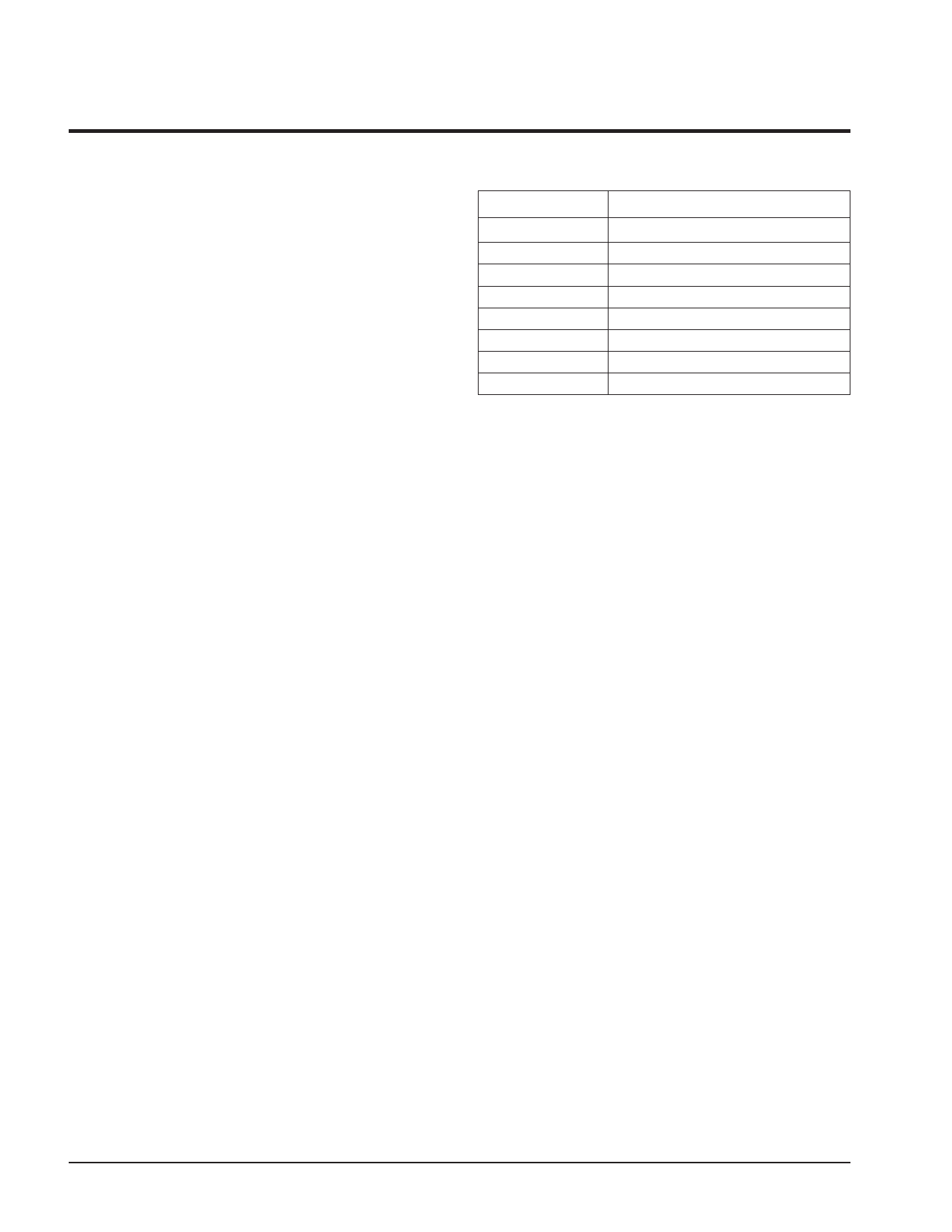
PIN NAMES
Symbol
A0–A17
I/O0–I/O7
WE
CE
OE
VCC
VSS
NC
Description
Address Inputs
Data Input/Output
Write Enable
Chip Enable
Output Enable
+5V
Ground
No Connect
3872 PGM T01
2
Share Link: 