ZXLD1352 データシートの表示(PDF) - Zetex => Diodes
部品番号
コンポーネント説明
メーカー
ZXLD1352 Datasheet PDF : 22 Pages
| |||
ZXLD1352
Absolute maximum ratings (voltages to GND unless otherwise stated)
Input voltage (VIN)
-0.3V to +30V (40V for 0.5 sec)
ISENSE voltage (VSENSE)
+0.3V to -5V (measured with respect to VIN)
LX output voltage (VLX)
-0.3V to +30V (40V for 0.5 sec)
Adjust pin input voltage (VADJ)
-0.3V to +6V
Switch output current (ILX)
500mA
Power dissipation (Ptot)
450mW
(Refer to package thermal de-rating curve on page 18)
Operating temperature (TOP)
-40 to 105°C
Storage temperature (TST)
-55 to 150°C
Junction temperature (Tj MAX)
150°C
These are stress ratings only. Operation above the absolute maximum rating may cause device failure. Operation at
the absolute maximum ratings, for extended periods, may reduce device reliability.
Thermal resistance
Junction to ambient (R⍜JA)
200°C/W
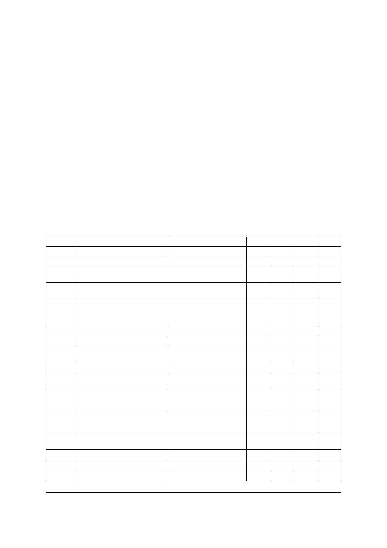
Electrical characteristics (test conditions: VIN=12V, Tamb=25°C unless otherwise stated) (*)
Symbol Parameter
Conditions
Min. Typ. Max. Unit
VIN
Input voltage
VSU
Internal regulator start-up threshold VIN rising
7
30 V
4.8
V
IINQoff
Quiescent supply current
with output off
ADJ pin grounded
20
30 µA
IINQon
Quiescent supply current
with output switching
ADJ pin floating
f=250kHz
250
500 µA
VSENSE
Mean current sense threshold
voltage
(defines LED current setting
accuracy)
Measured on ISENSE pin with
95
respect to VIN
VADJ =1.25V
100
105 mV
VSENSEHYS Sense threshold hysteresis
ISENSE
ISENSE pin input current
VREF
Internal reference voltage
VSENSE =VIN -0.1
Measured on ADJ pin with
pin floating
±15
%
1.25
10 µA
1.21
1.25
1.29 V
⌬VREF /⌬T
VADJ
Temperature coefficient of VREF
External control voltage range on
ADJ pin for dc brightness control (†)
50
ppm/°C
0.3
2.5 V
VADJoff
DC voltage on ADJ pin to switch
device from active (on) state to
quiescent (off) state
VADJ falling
0.15
0.2
0.25 V
VADJon
DC voltage on ADJ pin to switch
device from quiescent (off) state to
active (on) state
VADJ rising
0.2
0.25
0.3 V
RADJ
ILXmean
RLX
Resistance between ADJ pin and
VREF
Continuous LX switch current
LX Switch ‘On’ resistance
35
65 k⍀
0.37 A
1.5
2⍀
ILX(leak)
LX switch leakage current
1 µA
Issue 1 - August 2008
2
© Diodes Incorporated 2008
www.zetex.com
www.diodes.com
Share Link: 