SMP9212 データシートの表示(PDF) - Summit Microelectronics
部品番号
コンポーネント説明
メーカー
SMP9212 Datasheet PDF : 13 Pages
| |||
SMP9210, SMP9211, SMP9212
Preliminary
DEVICE OPERATION
INTRODUCTION
ACCESSING THE DACS
The device has two 10-Bit digital to analog converters that
are comprised of a resistor network that converts a digital
input into an equivalent analog output voltage in proportion
to the applied reference voltage. The voltage differential
between each of the VREFL and VREFH input pairs sets the
full-scale output voltage for their respective DAC.
Each DAC has a 10-Bit volatile register that holds the
current digital value. The register can be set to any value
by the serial interface; commanded to load the zero scale
value, full scale value or mid-scale value; or can recall a
preset value stored in a nonvolatile register.
Each DAC has a 10-Bit nonvolatile register that can hold
a ‘set-and-forget’ value that can be recalled whenever the
device is powered-on.
The device also has a nonvolatile configuration register
that is accessible over the 2-wire bus. The configuration
register is used to select the device type identifier, the
function of pin 8 and the DAC power-on state.
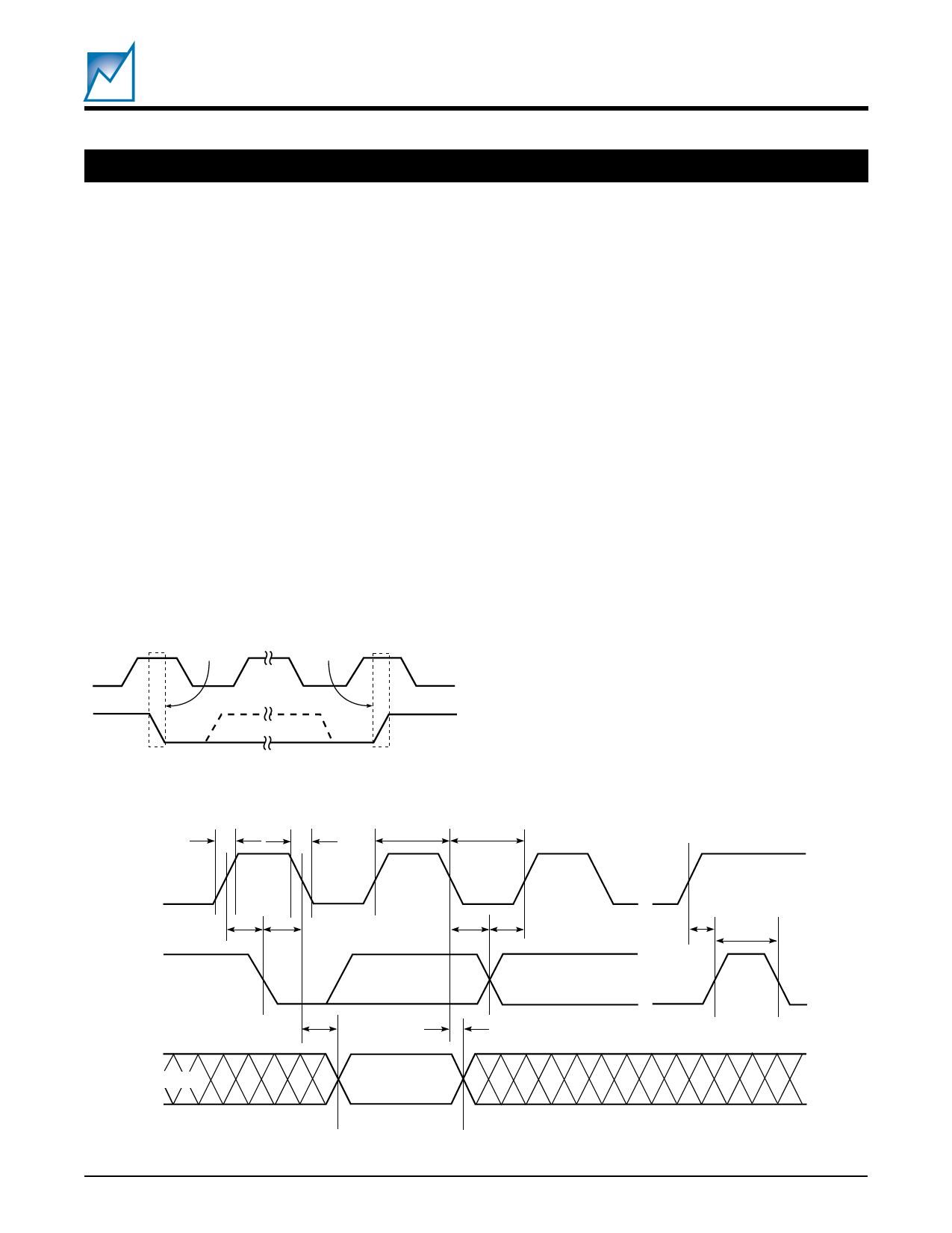
SCL
SDA In
START
Condition
STOP
Condition
The device uses the industry standard 2-wire serial proto-
col. The bus is designed for two-way, two-line serial
communication between different integrated circuits. The
two lines are the SCL (serial clock) and SDA (serial data)
and both lines must be tied to the positive supply through
a pull-up resistor. The protocol defines devices as being
either Masters or Slaves. The SMP9210, -11, or -12 will
always be a Slave because it does not initiate any
communications or provide a clock output.
Data transfers are initiated when a Master issues a Start
condition, which is a high to low transition on SDA while
SCL is high (see Figure 1). The Start is immediately
followed by an eight bit transmission: bits 7 through 1
comprise the device type identifier and bus device bus
address; bit 0 is the Read/Write bit indicating the action
to follow. If the intended device receives the byte and
recognizes its address it will return an Acknowledge
during the 9th clock cycle. Some data transfers will be
concluded with a Stop condition, which is a low to high
transition on SDA while SCL is high. Note: a Stop
condition must be performed for all nonvolatile Write
operations. Timing for all I2C operations are summarized
in Figure 2 and Table 1.
The DAC device type identifier default is 0101BIN. In order
to accommodate more than eight devices on a single bus
the device type identifier can be modified by the end user
by writing to the Configuration Registers. (See page 10)
2048 Fig01
Figure 1. START and STOP Timing
tR
tF
tHIGH
tLOW
SCL
tSU:STA
SDA In
tHD:STA
tHD:DAT
tSU:DAT
tSU:STO
tBUF
tAA
tDH
SDA Out
SUMMIT MICROELECTRONICS, Inc.
Figure 2. Data/Clock Timing
2048 3.3 10/03/01
2048 Fig02
7
Share Link: 