DAC8222GP データシートの表示(PDF) - Analog Devices
部品番号
コンポーネント説明
メーカー
DAC8222GP Datasheet PDF : 15 Pages
| |||
DAC8222
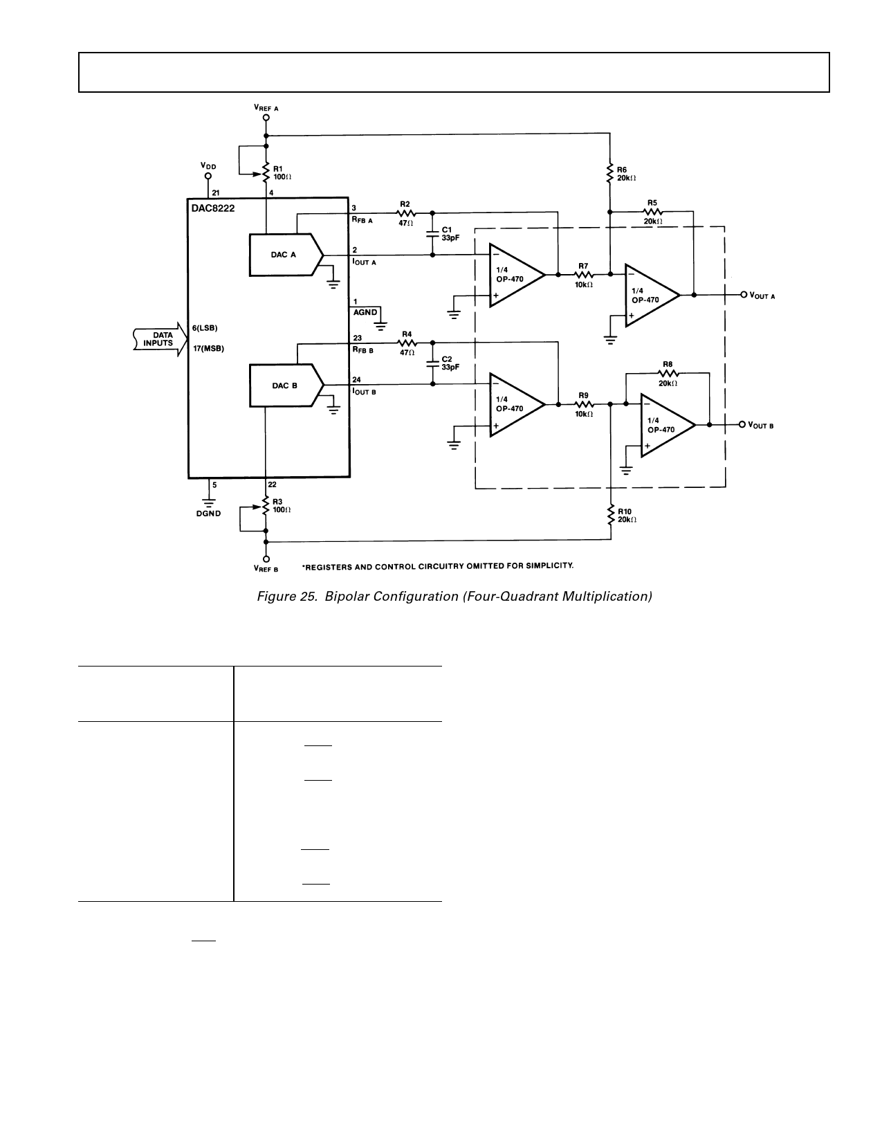
Figure 25. Bipolar Configuration (Four-Quadrant Multiplication)
Table III. Bipolar (Offset Binary) Code Table
(Refer to Figure 25)
Binary Number in
DAC Register
MSB
LSB
Analog Output, VOUT
(DAC A or DAC B)
1111 1111 1111
1000 0000 0001
2047
+VREF 2048
1
+VREF 2048
1000 0000 0000
0V
0111 1111 1111
0000 0000 0000
1
–VREF 2048
2048
–VREF 2048
NOTE
1
1 LSB = (2–11) (VREF) = 2048 (VREF)
resistors R5, R6, R7, should be ratio-matched to 0.01% so that
gain error meets data sheet specifications. (Corresponding resis-
tors, R8, R9, and R10 for DAC B should also be matched to
0.01%). The resistors should have identical temperature coeffi-
cients if operating over the full temperature range.
Zero and full-scale are adjusted one of two ways and are at the
user’s discretion. Zero-output can be adjusted by first setting
the digital inputs to 1000 0000 0000 and adjusting R1 (R3 for
DAC B) so that VOUTA (or VOUT B) equals 0 V. If R1, R2 (R3,
R4 for DAC B) are omitted, then VOUT = 0 V can be adjusted
by varying R6, R7 (R9, R10 for DAC B) ratios. Full-scale is ad-
justed by setting the digital inputs to 1111 1111 1111 and vary-
ing R5 (R8 for DAC B). Full-scale can also be adjusted by
varying VREF. Full-scale output is equal to VREF minus one LSB.
REV. C
–11–
Share Link: 