DAC8222EW データシートの表示(PDF) - Analog Devices
部品番号
コンポーネント説明
メーカー
DAC8222EW Datasheet PDF : 15 Pages
| |||
DAC8222
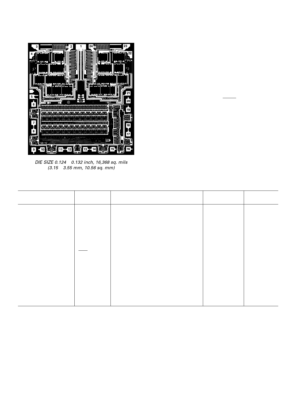
DICE CHARACTERISTICS
11. AGND
12. IOUT A
13. RFB A
14. VREF A
15. DGND
16. DB11(MSB)
17. DB10
18. DB9
19. DB8
10. DB7
11. DB6
12. DB5
13. DB4
14. DB3
15. DB2
16. DB1
17. DB0 (LSB)
18. DAC A/DAC B
19. LDAC
20. WR
21. VDD
22. VREF B
23. RFB B
24. IOUT B
Substrate (die backside) is internally connected to VDD.
DIE SIZE 0.124 × 0.132 inch, 16,368 sq. mils
(3.15 × 3.55 mm, 10.56 sq. mm)
WAFER TEST LIMITS (@ VDD = +5 V or +15 V, VREF A = VREF B = +10 V, VOUT A = VOUT B = 0 V; AGND = DGND = 0 V; TA = +25؇C)
Parameter
Symbol
Conditions
DAC8222G
Limit
Units
Relative Accuracy
Differential Nonlinearity
Full Scale Gain Error1
Output Leakage
(IOUT A, IOUT B)
Input Resistance
(VREF A, VREF B)
Input Resistance Match
Digital Input High
Digital Input Low
Digital Input Current
Supply Current
DC Supply Rejection
(∆Gain/∆VDD)
INL
DNL
GFSE
ILKG
RREF
∆RREF
RREF
VINH
VINL
IIN
IDD
PSR
Endpoint Linearity Error
All Grades are Guaranteed Monotonic
Digital Inputs = 1111 1111 1111
Digital Inputs = 0000 0000 0000
Pads 2 and 24
Pads 4 and 22
VDD = +5 V
VDD = +15 V
VDD = +5 V
VDD = +15 V
VIN = 0 V or VDD; VINL or VINH
All Digital Inputs VINL or VINH
All Digital Inputs 0 V or VDD
∆VDD = ± 5%
±1
±1
±4
± 50
8/15
±1
2.4
13.5
0.8
1.5
±1
2
0.1
0.002
LSB max
LSB max
LSB max
nA max
kΩ max
% max
V min
V min
V max
V min
µA max
mA max
%/% max
NOTES
1Measured using internal RFB A and RFB B.
Electrical tests are performed at wafer probe to the limits shown. Due to variations in assembly methods and normal yield loss, yield after packaging is not guaranteed
for standard product dice. Consult factory to negotiate specifications based on dice lot qualification through sample lot assembly and testing.
–4–
REV. C
Share Link: 