DAC8222FP データシートの表示(PDF) - Analog Devices
部品番号
コンポーネント説明
メーカー
DAC8222FP Datasheet PDF : 15 Pages
| |||
DAC8222
between IOUT and AGND terminals be as close to zero as practi-
cal in order to keep DAC errors to a minimum. This is normally
done by connecting AGND to the noninverting input of an op
amp and IOUT to the inverting input. The DAC’s internal resis-
tor (RFB) can be used for the feedback resistor by connecting the
op amp’s output directly to the DAC’s RFB terminal. The op
amp also provides the current-to-voltage conversion for the
DAC’s output current. The output voltage is dependent on the
DAC’s digital input code and VREF, and is given by:
VOUT = –VREF × D/4096
where D is the digital input code integer number that is between
0 and 4095.
The DAC’s input resistance, VREF (Figure 19), is always equal
to a constant value, R. This means that VREF can be driven by a
reference voltage or current, ac or dc (positive or negative). It is
recommended that a low-temperature-coefficient external RFB
resistor be used if a current source is employed.
The DAC’s output capacitance (COUT) is code dependent and
varies from 90 pF (all digital inputs low) to 120 pF (all digital
inputs high).
Figure 19 shows a transistor switch in series with the R-2R lad-
der terminating resistor and RFB resistor. They were designed
into the DAC to binarily match the ladder leg switches and im-
prove power supply rejection and gain error temperature coeffi-
cient. The gates of these transistor switches are connected to
VDD, so that an “open-circuit” exists when VDD is not applied.
This means that an op amp’s output voltage will go to either
“rail” if powered up before the DAC. Also, RFB resistance can-
not be measured without VDD being applied.
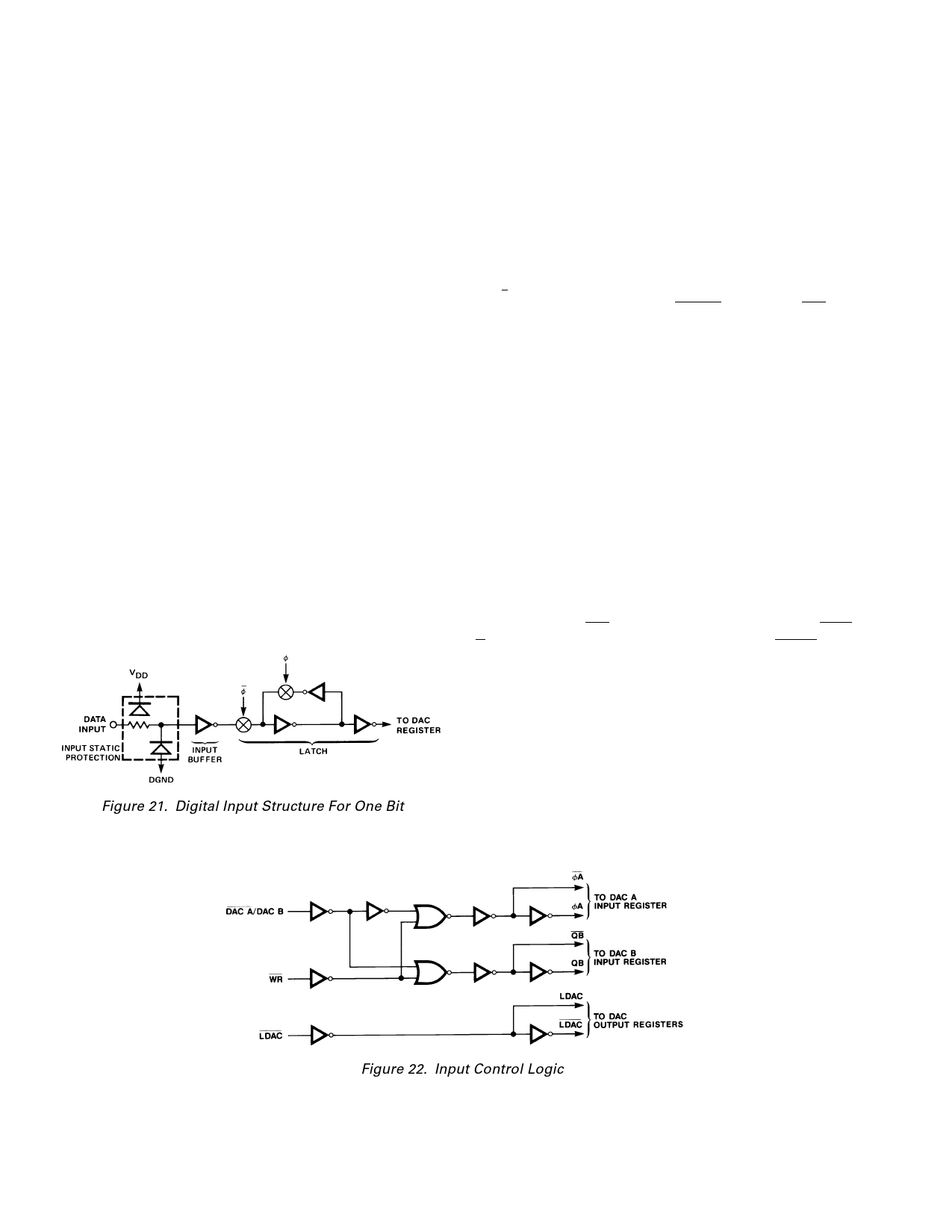
Figure 21. Digital Input Structure For One Bit
DIGITAL SECTION
The DAC8222’s digital inputs are CMOS inserters. They were
designed to convert TTL and CMOS input logic levels into
voltage levels to drive the internal circuitry. The digital inputs
are TTL compatible at VDD = +5 V and CMOS compatible at
VDD = +15 V. The DAC8222 can use +5 V CMOS logic levels
with VDD = +12 V; however, supply current will rise to approxi-
mately 5 mA–6 mA.
Figure 21 shows the DAC’s digital input register structure for
one bit. This circuit drives the DAC register. Digital controls φ
and φ shown are generated from DAC A/DAC B and WR con-
trol signals.
As shown in Figure 21, these inputs are electrostatic-discharge
protected with two internal distributed diodes; they are con-
nected between VDD and DGND. Each digital input has a typi-
cal input current of less than 1 nA.
When the digital inputs are in the region of +1.2 V to +2.8 V
(peaking at +1.8 V) using a +5 V power supply or in the region
of +1.7 V to +12 V (peaking at +3.9 V) with a +15 V power
supply, the input register transistors are operating in their linear
region and draw current from the power supply. It is therefore,
recommended that the digital input voltages be as close to the
supply rails (VDD and DGND) as is practically possible to keep
supply currents at a minimum. The DAC8222 may be operated
with any supply voltage between the range of +5 V to +15 V.
INTERFACE CONTROL LOGIC
The DAC8222’s input control logic circuitry is shown in Figure
22. Note how the WR signal is used in conjunction with DAC
A/ DAC B to load data into either input register. LDAC loads
data from the input registers to the DAC register; the DAC’s
analog output voltage is determined by the data contained in
each DAC register.
The truth table for the DAC registers is shown in the Mode Se-
lection Table. Note how the input register is transparent when
WR is low and LDAC is high, and that the DAC register is
transparent when WR is high and LDAC is low (LDAC updates
the DAC’s analog output voltage). The DAC is transparent
from input to output when WR and LDAC are both low, and
the DAC is latched (input and output is not being updated)
when WR and LDAC are both high.
Figure 22. Input Control Logic
–8–
REV. C
Share Link: 