MC74VHC139DTEL データシートの表示(PDF) - ON Semiconductor
部品番号
コンポーネント説明
メーカー
MC74VHC139DTEL Datasheet PDF : 8 Pages
| |||
MC74VHC139
ÎÎÎÎÎÎÎÎÎÎÎÎÎÎÎÎÎÎÎÎÎÎÎ MAXIMUM RATINGS*
ÎÎÎÎÎÎÎÎÎÎÎÎÎÎÎÎÎÎÎÎÎÎÎ Symbol
Parameter
Value
Unit
ÎÎÎÎÎÎÎÎÎÎÎÎÎÎÎÎÎÎÎÎÎÎÎ VCC DC Supply Voltage
– 0.5 to + 7.0
V
ÎÎÎÎÎÎÎÎÎÎÎÎÎÎÎÎÎÎÎÎÎÎÎ Vin DC Input Voltage
– 0.5 to + 7.0
V
ÎÎÎÎÎÎÎÎÎÎÎÎÎÎÎÎÎÎÎÎÎÎÎ Vout DC Output Voltage
– 0.5 to VCC + 0.5 V
ÎÎÎÎÎÎÎÎÎÎÎÎÎÎÎÎÎÎÎÎÎÎÎ IIK Input Diode Current
– 20
mA
ÎÎÎÎÎÎÎÎÎÎÎÎÎÎÎÎÎÎÎÎÎÎÎ IOK Output Diode Current
± 20
mA
ÎÎÎÎÎÎÎÎÎÎÎÎÎÎÎÎÎÎÎÎÎÎÎ Iout DC Output Current, per Pin
± 25
mA
ÎÎÎÎÎÎÎÎÎÎÎÎÎÎÎÎÎÎÎÎÎÎÎ ICC DC Supply Current, VCC and GND Pins
± 75
mA
ÎÎÎÎÎÎÎÎÎÎÎÎÎÎÎÎÎÎÎÎÎÎÎ PD Power Dissipation in Still Air,
SOIC Packages†
500
mW
TSSOP Package†
450
ÎÎÎÎÎÎÎÎÎÎÎÎÎÎÎÎÎÎÎÎÎÎÎ Tstg Storage Temperature
– 65 to + 150
_C
ÎÎÎÎÎÎÎÎÎÎÎÎÎÎÎÎÎÎÎÎÎÎÎÎÎÎÎÎÎÎÎÎÎÎÎÎÎÎÎÎÎÎÎÎÎÎ * Absolute maximum continuous ratings are those values beyond which damage to the device
may occur. Exposure to these conditions or conditions beyond those indicated may
adversely affect device reliability. Functional operation under absolute–maximum–rated
conditions is not implied.
†Derating — SOIC Packages: – 7 mW/_C from 65_ to 125_C
TSSOP Package: – 6.1 mW/_C from 65_ to 125_C
This device contains protection
circuitry to guard against damage
due to high static voltages or electric
fields. However, precautions must
be taken to avoid applications of any
voltage higher than maximum rated
voltages to this high–impedance cir-
cuit. For proper operation, Vin and
Vout should be constrained to the
range GND v (Vin or Vout) v VCC.
Unused inputs must always be
tied to an appropriate logic voltage
level (e.g., either GND or VCC).
Unused outputs must be left open.
RECOMMENDED OPERATING CONDITIONS
ÎÎÎÎÎÎÎÎÎÎÎÎÎÎÎÎÎÎÎÎÎÎÎ Symbol
Parameter
Min Max Unit
ÎÎÎÎÎÎÎÎÎÎÎÎÎÎÎÎÎÎÎÎÎÎÎ VCC DC Supply Voltage
ÎÎÎÎÎÎÎÎÎÎÎÎÎÎÎÎÎÎÎÎÎÎÎ Vin
DC Input Voltage
ÎÎÎÎÎÎÎÎÎÎÎÎÎÎÎÎÎÎÎÎÎÎÎ Vout DC Output Voltage
ÎÎÎÎÎÎÎÎÎÎÎÎÎÎÎÎÎÎÎÎÎÎÎ TA
Operating Temperature
ÎÎÎÎÎÎÎÎÎÎÎÎÎÎÎÎÎÎÎÎÎÎÎ tr, tf
Input Rise and Fall Time
ÎÎÎÎÎÎÎÎÎÎÎÎÎÎÎÎÎÎÎÎÎÎÎÎÎÎÎÎÎÎÎÎÎÎÎÎÎÎÎÎÎÎÎÎÎÎ (Figure 1)
VCC = 3.3V ±0.3V
VCC =5.0V ±0.5V
2.0
0
0
– 55
0
0
5.5 V
5.5 V
VCC
V
+ 125 _C
100 ns/V
20
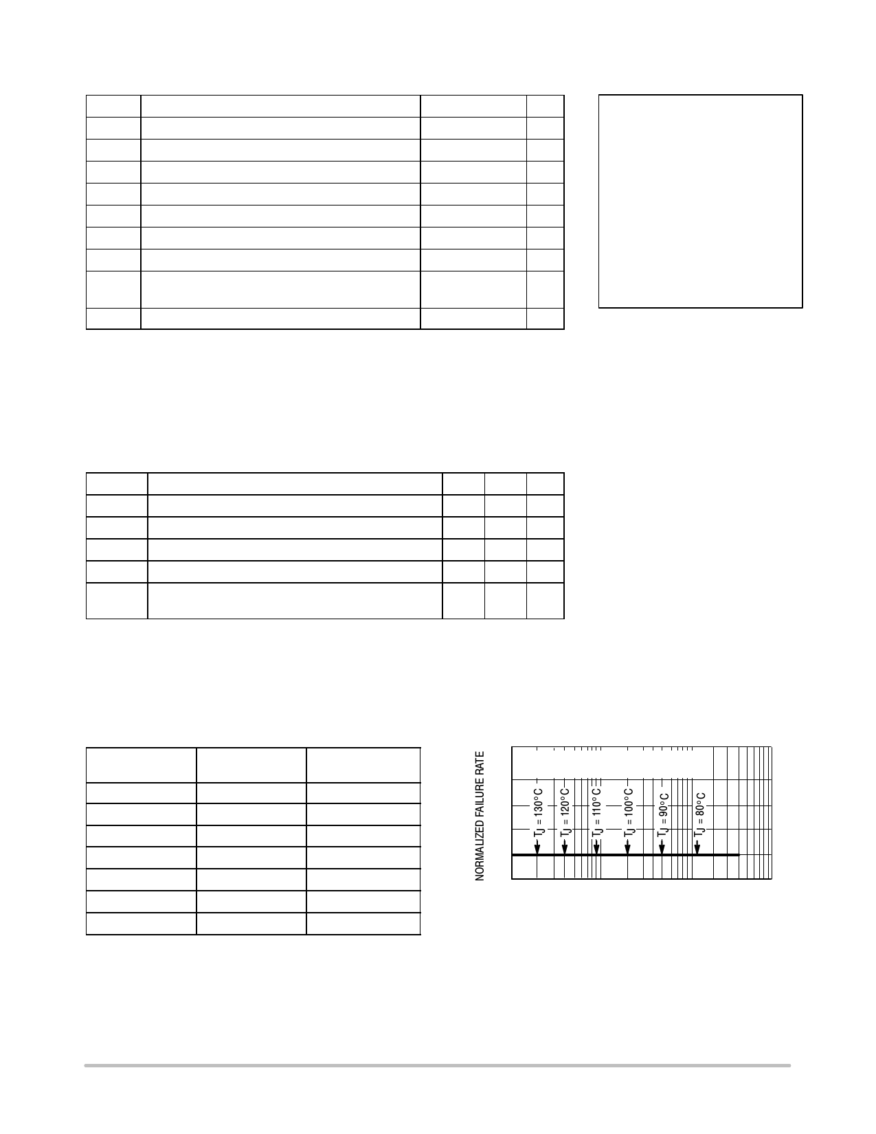
The qJA of the package is equal to 1/Derating. Higher junction temperatures may affect the expected lifetime of the device per the table and
figure below.
DEVICE JUNCTION TEMPERATURE VERSUS
TIME TO 0.1% BOND FAILURES
Junction
Temperature °C
80
90
100
110
120
130
140
Time, Hours
1,032,200
419,300
178,700
79,600
37,000
17,800
8,900
Time, Years
117.8
47.9
20.4
9.4
4.2
2.0
1.0
FAILURE RATE OF PLASTIC = CERAMIC
UNTIL INTERMETALLICS OCCUR
1
1
10
100
1000
TIME, YEARS
Figure 2. Failure Rate vs. Time
Junction Temperature
http://onsemi.com
4
Share Link: 