IR2S1844PBF データシートの表示(PDF) - International Rectifier
部品番号
コンポーネント説明
メーカー
IR2S1844PBF Datasheet PDF : 26 Pages
| |||
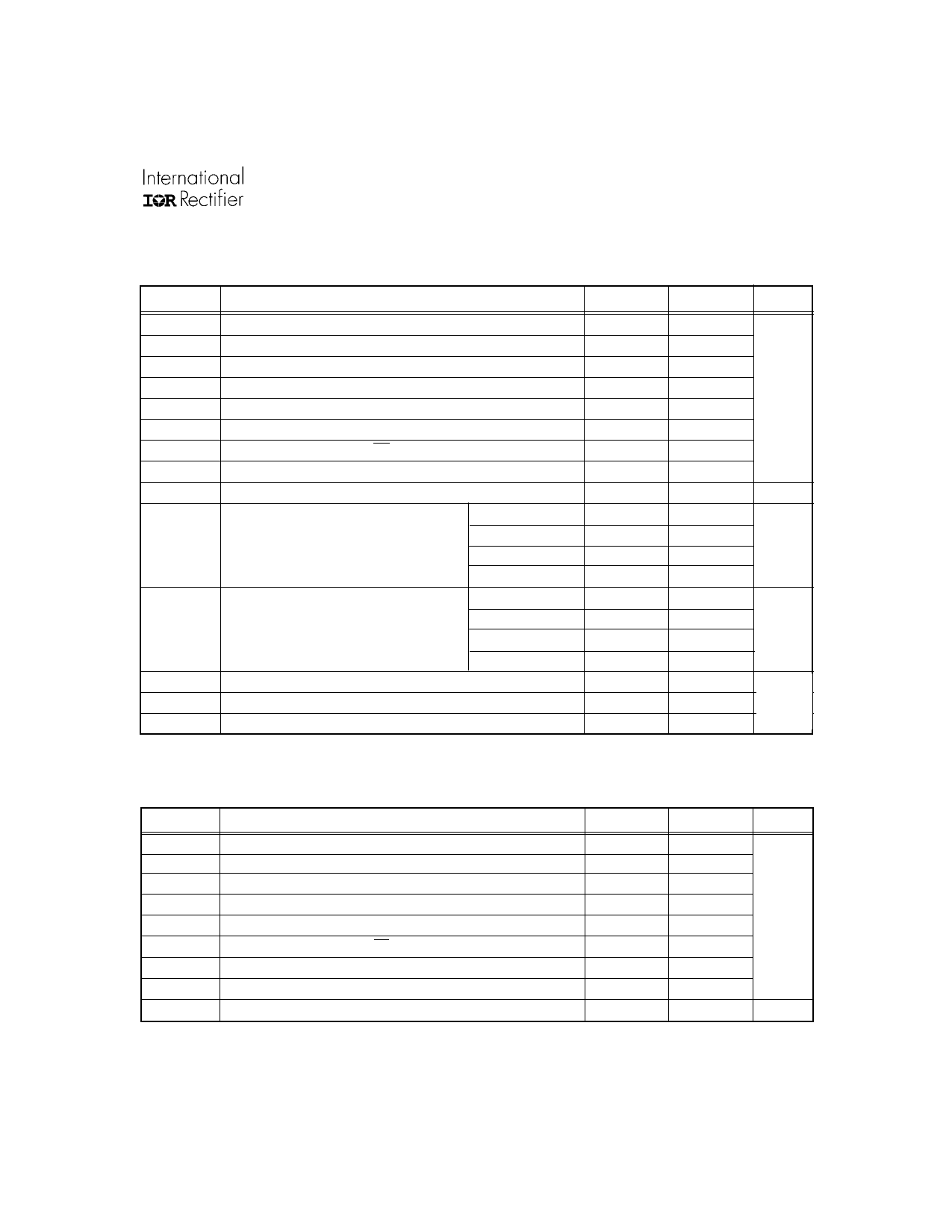
IRS2184/IRS21844(S)PbF
Absolute Maximum Ratings
Absolute maximum ratings indicate sustained limits beyond which damage to the device may occur. All voltage parameters
are absolute voltages referenced to COM. The thermal resistance and power dissipation ratings are measured under board
mounted and still air conditions.
Symbol
Definition
Min.
Max. Units
VB
VS
VHO
VCC
VLO
DT
VIN
VSS
dVS/dt
High-side floating absolute voltage
High-side floating supply offset voltage
High-side floating output voltage
Low-side and logic fixed supply voltage
Low-side output voltage
Programmable deadtime pin voltage (IRS21844 only)
Logic input voltage (IN & SD)
Logic ground (IRS21844 only)
Allowable offset supply voltage transient
(8-lead PDIP)
-0.3
VB - 20
VS - 0.3
-0.3
-0.3
VSS - 0.3
VSS - 0.3
VCC - 20
—
—
620 (Note 1)
VB + 0.3
VB + 0.3
20 (Note 1)
VCC + 0.3
VCC + 0.3
VCC + 0.3
VCC + 0.3
50
1.0
V
V/ns
(8-lead SOIC)
—
PD
Package power dissipation @ TA ≤ +25 °C
(14-lead PDIP)
—
0.625
1.6
W
(14-lead SOIC)
—
1.0
(8-lead PDIP)
—
125
(8-lead SOIC)
—
RthJA
Thermal resistance, junction to ambient
(14-lead PDIP)
—
200
75
°C/W
(14-lead SOIC)
—
120
TJ
Junction temperature
—
150
TS
Storage temperature
-50
150
°C
TL
Lead temperature (soldering, 10 seconds)
—
300
Note 1: All supplies are fully tested at 25 V and an internal 20 V clamp exists for each supply.
Recommended Operating Conditions
The input/output logic timing diagram is shown in Fig. 1. For proper operation the device should be used within the
recommended conditions. The VS and VSS offset rating are tested with all supplies biased at a 15 V differential.
Symbol
Definition
Min.
Max. Units
VB
High-side floating supply absolute voltage
VS
High-side floating supply offset voltage
VHO
High-side floating output voltage
VCC
Low-side and logic fixed supply voltage
VLO
Low-side output voltage
VIN
Logic input voltage (IN & SD)
DT
Programmable deadtime pin voltage (IRS21844 only)
VSS
Logic ground (IRS21844 only)
TA
Ambient temperature
VS + 10
Note 2
VS + 20
600
VS
VB
10
20
0
VCC
V
VSS
VCC
VSS
VCC
-5
5
-40
125
°C
Note 2: Logic operational for VS of -5 V to +600 V. Logic state held for VS of -5 V to -VBS. (Please refer to the Design Tip
DT97-3 for more details).
www.irf.com
2
Share Link: 