SST25PF080B データシートの表示(PDF) - Microchip Technology
部品番号
コンポーネント説明
メーカー
SST25PF080B Datasheet PDF : 32 Pages
| |||
SST25PF080B
4.2 Write Protection
SST25PF080B provides software Write protection. The
Write Protect pin (WP#) enables or disables the lock-
down function of the status register. The Block-Protec-
tion bits (BP2, BP1, BP0, and BPL) in the status regis-
ter provide Write protection to the memory array and
the status register. See Table 4-3 for the Block-Protec-
tion description.
4.2.1 WRITE PROTECT PIN (WP#)
The Write Protect (WP#) pin enables the lock-down
function of the BPL bit (bit 7) in the status register.
When WP# is driven low, the execution of the Write-
Status-Register (WRSR) instruction is determined by
the value of the BPL bit (see Table 4-1). When WP# is
high, the lock-down function of the BPL bit is disabled.
TABLE 4-1: CONDITIONS TO EXECUTE WRITE-STATUS-REGISTER (WRSR) INSTRUCTION
WP#
BPL
Execute WRSR Instruction
L
1
Not Allowed
L
0
Allowed
H
X
Allowed
4.3 Security ID
SST25PF080B offers a 256-bit Security ID (Sec ID)
feature. The Security ID space is divided into two parts
– one factory-programmed, 64-bit segment and one
user-programmable 192-bit segment. The factory-pro-
grammed segment is programmed at Microchip with a
unique number and cannot be changed. The user-pro-
grammable segment is left unprogrammed for the cus-
tomer to program as desired.
Use the Program SID command to program the Secu-
rity ID using the address shown in Table 4-5. Once pro-
grammed, the Security ID can be locked using the
Lockout SID command. This prevents any future write
to the Security ID.
The factory-programmed portion of the Security ID can
never be programmed, and none of the Security ID can
be erased.
4.4 Status Register
The software status register provides status on
whether the flash memory array is available for any
Read or Write operation, whether the device is Write
enabled, and the state of the Memory Write protection.
During an internal Erase or Program operation, the sta-
tus register may be read only to determine the comple-
tion of an operation in progress. Table 4-2 describes
the function of each bit in the software status register.
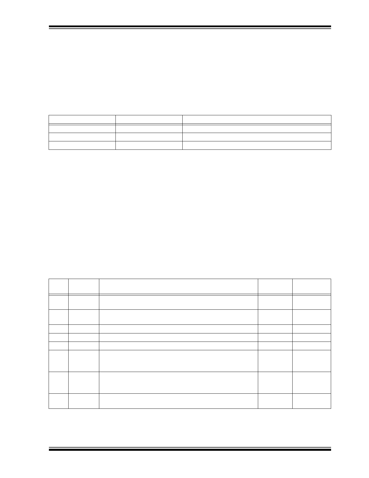
TABLE 4-2: SOFTWARE STATUS REGISTER
Bit Name
0 BUSY
1 WEL
2 BP0
3 BP1
4 BP2
5 SEC1
6 AAI
7 BPL
Function
1 = Internal Write operation is in progress
0 = No internal Write operation is in progress
1 = Device is memory Write enabled
0 = Device is not memory Write enabled
Indicates current level of block write protection
Indicates current level of block write protection
Indicates current level of block write protection
Security ID status
1 = Security ID space locked
0 = Security ID space not locked
Auto Address Increment Programming status
1 = AII programming mode
0 = Byte-Program mode
1 = BP2, BP1, BP0 are read-only bits
0 = BP2, BP1, BP0 are readable/writable
Default at
Power-up
0
Read/Write
R
0
R
1
R/W
1
R/W
1
R/W
0 or 1
R
0
R
0
R/W
1. The Security ID status will always be ‘1’ at power-up after a successful execution of the Lockout SID instruction; otherwise,
the default at power-up is ‘0’.
2012 Microchip Technology Inc.
DS25134A-page 5
Share Link: 