82C52 データシートの表示(PDF) - Intersil
部品番号
コンポーネント説明
メーカー
82C52 Datasheet PDF : 20 Pages
| |||
82C52
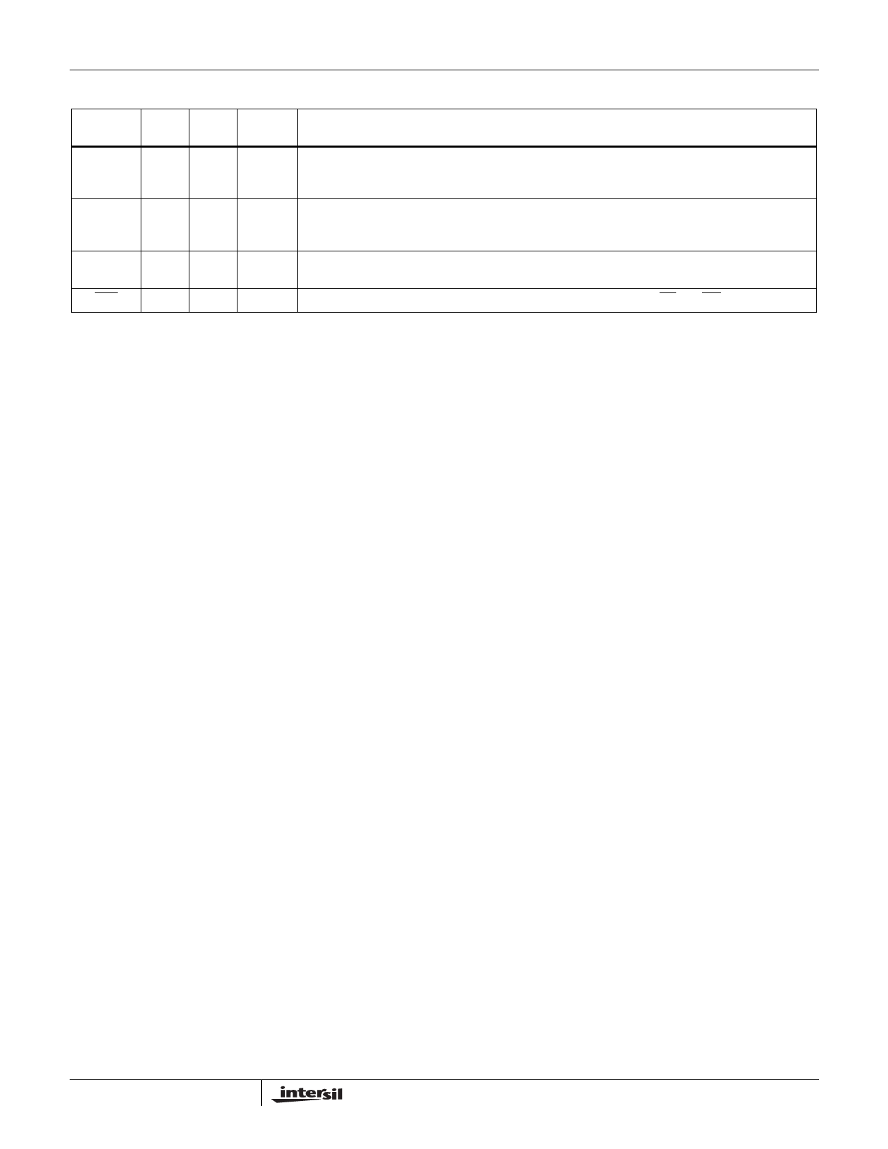
Pin Description (Continued)
PIN
ACTIVE
SYMBOL NO. TYPE LEVEL
DESCRIPTION
SDI
25
I
High SERIAL DATA INPUT: Serial data input to the 82C52 receiver circuits. A Mark (1) is high, and a
Space (0) is low. Data inputs on SDI are disabled when operating in the loop mode or when RST is
true.
DR
VCC
26
O
High DATA READY: A true level indicates that a character has been received, transferred to the RBR, and
is ready for transfer to the CPU. DR is reset on a data READ of the Receiver Buffer Register (RBR)
or when RST is true.
27
High VCC: +5V positive power supply pin. A 0.1µF decoupling capacitor from VCC (Pin 27) to GND (Pin
16) is recommended.
CS0
28
I
Low CHIP SELECT: The chip select input acts as an enable signal for the RD and WR input signals.
4
FN2950.3
April 26, 2006
Share Link: 