3054 データシートの表示(PDF) - Intersil
部品番号
コンポーネント説明
メーカー
3054 Datasheet PDF : 8 Pages
| |||
CA3054
Absolute Maximum Ratings TA = 25°C
Collector-to-Emitter Voltage, VCEO . . . . . . . . . . . . . . . . . . . . . . 15V
Collector-to-Base Voltage, VCBO. . . . . . . . . . . . . . . . . . . . . . . . 20V
Collector-to-Substrate Voltage, VCIO (Note 1) . . . . . . . . . . . . . . 20V
Emitter-to-Base Voltage, VEBO . . . . . . . . . . . . . . . . . . . . . . . . . . 5V
Collector Current, IC . . . . . . . . . . . . . . . . . . . . . . . . . . . . . . . . 50mA
Operating Conditions
Temperature Range . . . . . . . . . . . . . . . . . . . . . . . . . . . . 0°C to 85°C
Thermal Information
Thermal Resistance (Typical, Note 2)
θJA (°C/W)
SOIC Package . . . . . . . . . . . . . . . . . . . . . . . . . . . . .
140
Maximum Junction Temperature (Die) . . . . . . . . . . . . . . . . . . . . 175°C
Maximum Junction Temperature (Plastic Package) . . . . . . . . 150°C
Maximum Storage Temperature Range . . . . . . . . . . -65°C to 150°C
Maximum Lead Temperature (Soldering 10s) . . . . . . . . . . . . 300°C
(Lead Tips Only)
Maximum Power Dissipation (Any One Transistor) . . . . . . . 300mW
CAUTION: Stresses above those listed in “Absolute Maximum Ratings” may cause permanent damage to the device. This is a stress only rating and operation of the
device at these or any other conditions above those indicated in the operational sections of this specification is not implied.
NOTES:
1. The collector of each transistor of the CA3054 is isolated from the substrate by an integral diode. The substrate must be connected to a voltage
which is more negative than any collector voltage in order to maintain isolation between transistors and provide for normal transistor action. The
substrate should be maintained at signal (AC) ground by means of a suitable grounding capacitor, to avoid undesired coupling between transistors.
2. θJA is measured with the component mounted on an evaluation PC board in free air.
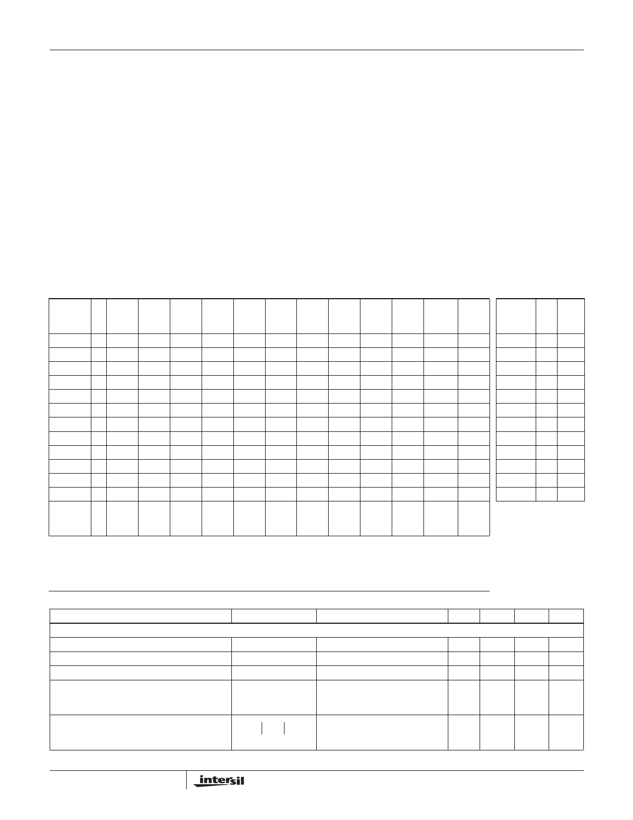
Maximum Voltage Ratings
The following chart gives the range of voltages which can be applied to the terminals listed vertically with respect to the termi-
nals listed horizontally. For example, the voltage range of the vertical Terminal 2 with respect to Terminal 4 is +15V to -5V.
(NOTE 4)
TERM
NO. 13 14
1
2
3
4
6
7
8
9
11
12
5
13
0, -20 Note 3 +5, -5 Note 3 +15, -5 Note 3 Note 3 Note 3 Note 3 Note 3 Note 3 Note 3
14
Note 3 Note 3 Note 3 +20, 0 Note 3 Note 3 Note 3 Note 3 Note 3 Note 3 +20, 0
1
+20, 0 Note 3 +20, 0 Note 3 Note 3 Note 3 Note 3 Note 3 Note 3 +20, 0
2
Note 3 +15, -5 Note 3 Note 3 Note 3 Note 3 Note 3 Note 3 Note 3
3
+1, -5 Note 3 Note 3 Note 3 Note 3 Note 3 Note 3 Note 3
4
Note 3 Note 3 Note 3 Note 3 Note 3 Note 3 Note 3
6
0, -20 Note 3 +5, -5 Note 3 +15, -5 Note 3
7
Note 3 Note 3 Note 3 Note 3 +20, 0
8
+20, 0 Note 3 Note 3 +20, 0
9
Note 3 +15, -5 Note 3
11
-1, -5 Note 3
12
Note 3
5
Ref.
Sub-
strate
NOTES:
3. Voltages are not normally applied between these terminals. Voltages appearing between these terminals will be safe
if the specified limits between all other terminals are not exceeded.
4. Terminal No. 10 of CA3054 is not used.
Maximum
Current Ratings
(NOTE 4)
TERM IIN IOUT
NO. mA mA
13
5 0.1
14 50 0.1
1
50 0.1
2
5 0.1
3
5 0.1
4
0.1 50
6
5 0.1
7
50 0.1
8
50 0.1
9
5 0.1
11
5 0.1
12 0.1 50
Electrical Specifications TA = 25°C
PARAMETER
SYMBOL
DC CHARACTERISTICS For Each Differential Amplifier
Input Offset Voltage (Figure 8)
Input Offset Current (Figure 9)
Input Bias Current (Figure 5)
Quiescent Operating Current Ratio
(Figure 5)
VIO
IIO
II
I--C-----(--Q----1----)
IC(Q2)
or
I--C-----(--Q----5----)
IC(Q6)
Temperature Coefficient Magnitude of
Input Offset Voltage (Figure 7)
--∆----V----I--O-----
∆T
TEST CONDITIONS
VCB = 3V, IE(Q3) = IE(Q4) = 2mA
VCB = 3V, IE(Q3) = IE(Q4) = 2mA
VCB = 3V, IE(Q3) = IE(Q4) = 2mA
VCB = 3V, IE(Q3) = IE(Q4) = 2mA
VCB = 3V, IE(Q3) = IE(Q4) = 2mA
MIN TYP MAX UNIT
-
0.45
5
mV
-
0.3
2
µA
-
10
24
µA
- 0.98 to -
-
1.02
-
1.1
-
µV/°C
2
Share Link: 