VSC7130RC データシートの表示(PDF) - Vitesse Semiconductor
部品番号
コンポーネント説明
メーカー
VSC7130RC Datasheet PDF : 22 Pages
| |||
Data Sheet
VSC7130
VITESSE
SEMICONDUCTOR CORPORATION
Dual Repeater/Retimer
for Fibre Channel and Gigabit Ethernet
Implementing reference clock distribution in multi-node systems can be difficult and expensive if optimal
signal quality is to be achieved. In order to reduce this burden, the VSC7130 has a flexible reference input
buffer which can be either single-ended TTL, or differential PECL. If single-ended TTL, REFI+ should be con-
nected to the clock source and REFI- should be left unconnected. REFI- is biased to VDD/2 for TTL thresh-
olds. If a PECL source is used, connect the positive side to REFI+ and the negative side to REFI-. In order to
provide the reference clock to multiple devices, a reference clock output, REFO+/-, is provided which is just a
PECL buffered version of REFI+/-. In this way, multiple VSC7130s may be daisy chained together with the
REFO driving the REFI of the next device. When REFO is driving REFI, a 100Ω resistor should be con-
nected between REFI+ and REFI-.
The reference clock is used by the clock multiplier unit (CMU) in order to generate the internal baud rate
clock. In order to maximize signal quality of the TX and SO outputs, the REFI input should be of the highest
quality possible with sharp edges and low jitter. Duty cycle distortion is not very important since only the rising
edge of REFI is used. The CMU is a high performance analog PLL which multiplies the reference clock fre-
quency by 20 or 10 depending on HALF/FULL.
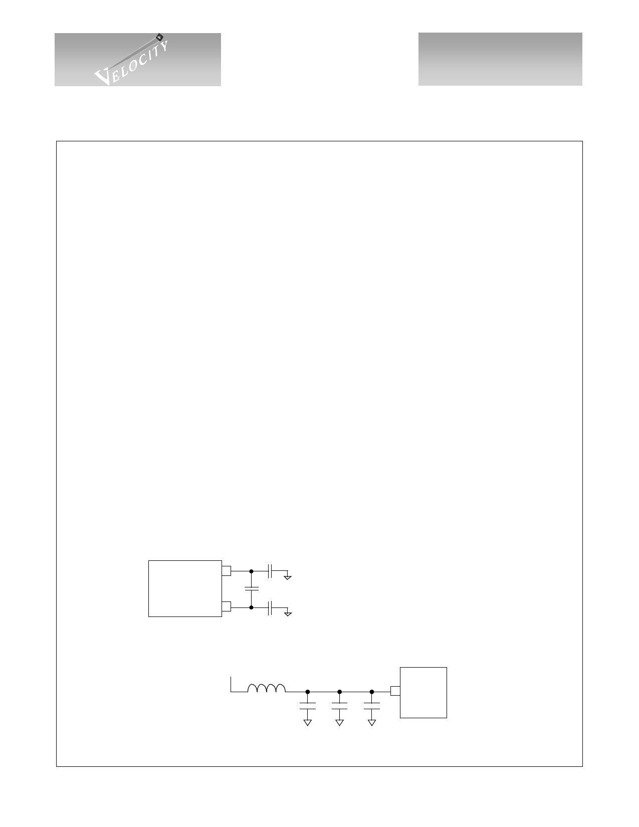
The on-chip PLL uses a single external 0.1µF capacitor, connected between CAP0 and CAP1, to control
the Loop Filter. This capacitor should be a multilayer ceramic dielectric, or better, with at least a 5V working
voltage rating and a good temperature coefficient, i.e. NPO is preferred but X7R is acceptable. These capacitors
are used to minimize the impact of common mode noise on the CMU, especially power supply noise. Higher
value capacitors provide better robustness in systems. NPO is preferred because if an X7R capacitor is used, the
power supply noise sensitivity will vary with temperature. For best noise immunity, the designer may use a
three capacitor circuit with one differential capacitor between CAP0 and CAP1, C1, a capacitor from CAP0 to
ground, C2, and a capacitor from CAP1 to ground, C3. Larger values are better but 0.1µF is adequate. However,
if the designer cannot use a three capacitor circuit, a single differential capacitor, C1, is adequate. These compo-
nents should be isolated from noisy traces. Figure 4 is the recommended Loop filtering scheme.
Separate power (VDDA) and ground (VSSA) are provided in order to allow a separately filtered power
supply to reduce noise. Figure 5 is the recommended VDDA filtering scheme.
Figure 4: Loop Filter Capacitors (Recommended Circuit)
CAP0
C2
C1
VSC7130
CAP1
C3
C1=C2=C3= >0.1µF
MultiLayer Ceramic
Surface Mount
NPO (Preferred) or X7R
5V Working Voltage Rating
Figure 5: VDDA Filtering (Recommended Circuit)
VDD
L1=Ferrite bead with
L1 C1
high impedance at high frequencies
and some DC resistance (0.5Ω)
C2 C3
VSSA
VSC7130
VDDA
C1=10-33µF
C2=0.1µF
C3=0.01µF-0.001µF
G52297-0, Rev 4.0
04/02/01
© VITESSE SEMICONDUCTOR CORPORATION • 741 Calle Plano • Camarillo, CA 93012
Tel: (800) VITESSE • FAX: (805) 987-5896 • Email: prodinfo@vitesse.com
Internet: www.vitesse.com
Page 5
Share Link: 