TDA1547 データシートの表示(PDF) - Philips Electronics
部品番号
コンポーネント説明
メーカー
TDA1547 Datasheet PDF : 18 Pages
| |||
Philips Semiconductors
Dual top-performance bitstream DAC
Product specification
TDA1547
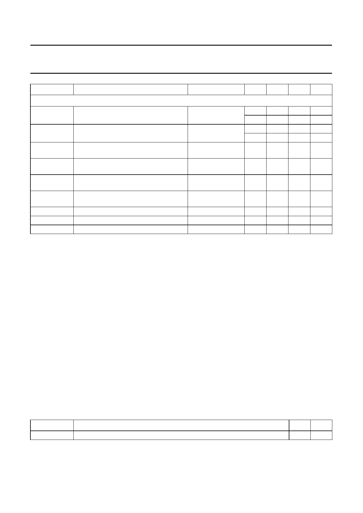
SYMBOL
PARAMETER
CONDITION
MIN TYP MAX UNIT
Supply current
(THD + N)/S THD + Noise; 0 dB
1 kHz; notes 2 and 3 −
−101 −96 dB
−
0.0009 0.0016 %
(THD + N)/S THD + Noise; 0 dB
f = 20 Hz to 20 kHz; −
−101 -
dB
notes 2 and 4
−
0.0009 -
%
(THD + N)/S THD + Noise; −20 dB
f = 1 kHz;
notes 2 and 3
−
−88 −84 dB
(THD + N)/S THD + Noise; −60 dB
f = 1 kHz;
notes 2 and 3
−
−48 −44 dB
S/N
signal-to-noise ratio
pattern 0101..;
notes 2 and 5
109 111 −
dB
S/N
signal-to-noise ratio; “A”-weighting
pattern 0101..;
−
113 −
dB
notes 2 and 5
fCLK
maximum clock frequency
α
channel separation
f = 1 kHz
−
−
10
101 115 −
MHz
dB
Tamb
operating ambient temperature
−20 −
70
°C
Notes to the quick reference data
1. Output level tracks linearly with both the clock frequency and the reference voltage (Vref L or Vref R).
2. Device measured in differential mode with external components as shown in Fig.5.
3. Measured with a one-bit data signal generated by the SAA7350 from an 8 fs (352.8 kHz), 20-bit, 1 kHz digital
sinewave. Measured over a 20 Hz to 20 kHz bandwidth.
4. Measured with a one-bit data signal generated by the SAA7350 from an 8 fs (352.8 kHz), 20-bit, 20 Hz to 20 kHz
digital sinewave. Measured over a 20 Hz to 20 kHz bandwidth.
5. The specified signal-to-noise ratio includes noise introduced by the application components as shown in Fig.5.
FUNCTIONAL DESCRIPTION
Both channels are completely separated to reach the desired high crosstalk suppression level.
Each channel consists of the following functional parts:
− One-bit input, which latches the incoming data to the system clock.
− Switch driver circuit, which generates the non-overlapping clock- and data-signals that control the DAC switched
capacitor networks.
− Switched capacitor network, this forms the actual DAC function, it supplies charge packets to the low-pass filter,
under control of the incoming one-bit code.
− Two high performance operational amplifiers, that perform the charge packet to voltage conversion and deliver a
differential output signal. The first pole of the low-pass filter is built around them.
THERMAL RESISTANCE
SYMBOL
Rth j-a
from junction to ambient
PARAMETER
MAX. UNIT
60
K/W
September 1991
6
Share Link: 