RF2416 データシートの表示(PDF) - RF Micro Devices
部品番号
コンポーネント説明
メーカー
RF2416 Datasheet PDF : 10 Pages
| |||
RF2416
Preliminary
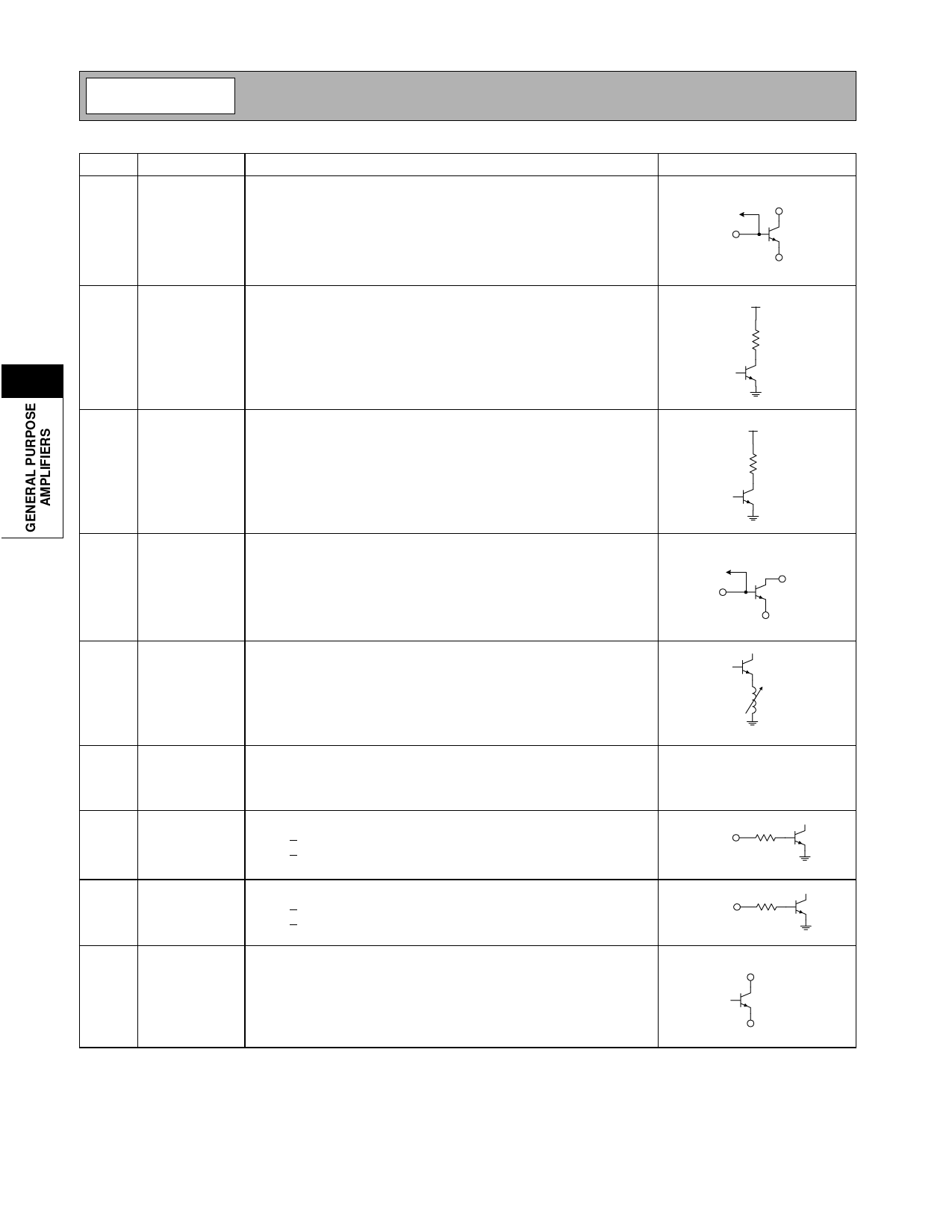
Pin Function Description
1
HB IN
DCS1800/PCS1900 RF input pin.
Interface Schematic
To Bias VCC1 HB
Circuit
HB IN
2
HB BIAS HB BIAS is set to the supply voltage at high gain mode. For bypass
mode see “Gain Select Possibility”.
HB GND1
HB VREF/P
4
3
LB BIAS LB BIAS is set to the supply voltage at high gain mode. For bypass
mode see “Gain Select Possibility”.
LB VREF/PD
4
LB IN
GSM900 RF input pin.
5
LB GND LNA emittance inductance. Total inductance is comprised of
package+bondwire+L2 on PCB.
To Bias
Circuit
LB IN
LB OUT
LB GND
6
LB OUT GSM900 Amplifier Output pin. This pin is an open-collector output. It
must be biased to VCC through a choke or matching inductor. This pin
is typically matched to 50Ω with a shunt bias/matching inductor and
series blocking/matching capacitor. Refer to application schematics.
7 LB SELECT This pin selects high gain and bypass for GSM900.
Select < 0.8V, high gain.
Select > 1.8V, low gain.
8 HB SELECT This pin selects high gain and bypass for DCS1800/PCS1900.
Select < 0.8V, high gain.
Select > 1.8V, low gain.
9
HB OUT DCS1800 Amplifier Output pin. This pin is an open-collector output. It
must be biased to VCC through a choke or matching inductor. This pin
is typically matched to 50Ω with a shunt bias/matching inductor and
series blocking/matching capacitor. Refer to application schematics.
LB SELECT
HB SELECT
HB OUT
HB GND2
4-202
Rev A2 010810
Share Link: 