2N5555 データシートの表示(PDF) - Motorola => Freescale
部品番号
コンポーネント説明
メーカー
2N5555 Datasheet PDF : 8 Pages
| |||
MOTOROLA
SEMICONDUCTOR TECHNICAL DATA
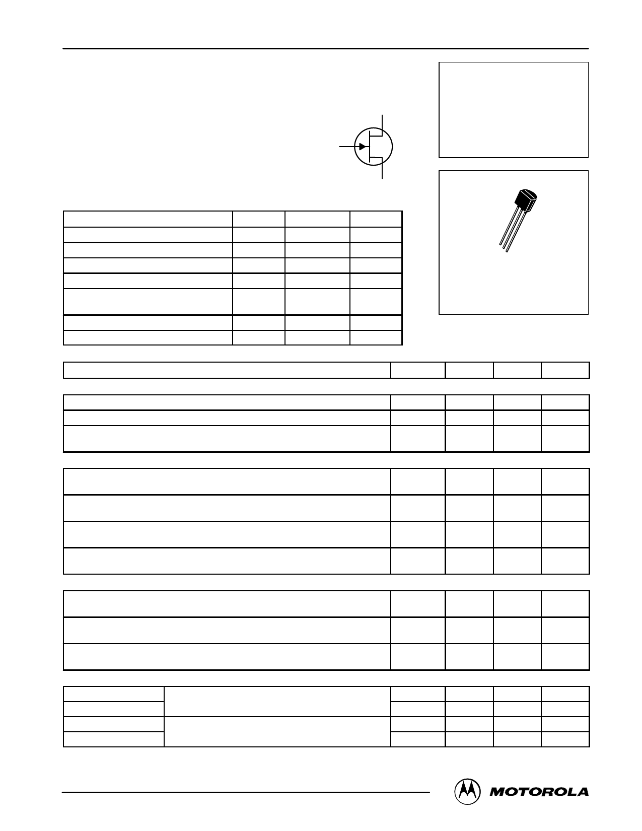
JFET Switching
N–Channel — Depletion
1 DRAIN
3
GATE
Order this document
by 2N5555/D
2N5555
2 SOURCE
MAXIMUM RATINGS
Rating
Symbol
Value
Unit
Drain – Source Voltage
Drain – Gate Voltage
Gate – Source Voltage
Forward Gate Current
Total Device Dissipation @ TC = 25°C
Derate above 25°C
VDS
VDG
VGS
IGF
PD
25
Vdc
25
Vdc
25
Vdc
10
mAdc
350
mW
2.8
mW/°C
Junction Temperature Range
TJ
– 65 to +150
°C
Storage Temperature Range
Tstg
– 65 to +150
°C
ELECTRICAL CHARACTERISTICS (TA = 25°C unless otherwise noted)
Characteristic
Symbol
OFF CHARACTERISTICS
Gate – Source Breakdown Voltage (IG = 10 µAdc, VDS = 0)
Gate Reverse Current (VGS = 15 Vdc, VDS = 0)
Drain Cutoff Current (VDS = 12 Vdc, VGS = – 10 V)
Drain Cutoff Current (VDS = 12 Vdc, VGS = – 10 V, TA = 100°C)
ON CHARACTERISTICS
Zero – Gate –Voltage Drain Current(1)
(VDS = 15 Vdc, VGS = 0)
Gate–Source Forward Voltage
(IG(f) = 1.0 mAdc, VDS = 0)
Drain–Source On–Voltage
(ID = 7.0 mAdc, VGS = 0)
Static Drain–Source On Resistance
(ID = 0.1 mAdc, VGS = 0)
SMALL– SIGNAL CHARACTERISTICS
V(BR)GSS
IGSS
ID(off)
IDSS
VGS(f)
VDS(on)
rDS(on)
Small–Signal Drain–Source “ON” Resistance
(VGS = 0, ID = 0, f = 1.0 kHz)
Input Capacitance
(VDS = 15 Vdc, VGS = 0, f = 1.0 MHz)
Reverse Transfer Capacitance
(VDS = 0, VGS = 10 Vdc, f = 1.0 MHz)
SWITCHING CHARACTERISTICS
rds(on)
Ciss
Crss
Turn–On Delay Time
Rise Time
(VDD = 10 Vdc, ID(on) = 7.0 mAdc,
VGS(on) = 0, VGS(off) = –10 Vdc) (See Figure 1)
Turn–Off Delay Time
Fall Time
(VDD = 10 Vdc, ID(on) = 7.0 mAdc,
VGS(on) = 0, VGS(off) = –10 Vdc) (See Figure 1)
1. Pulse Test: Pulse Width < 300 µs, Duty Cycle < 3.0%.
td(on)
tr
td(off)
tf
1
2
3
CASE 29–04, STYLE 5
TO–92 (TO–226AA)
Min
Max
Unit
25
—
Vdc
—
1.0
nAdc
—
10
nAdc
—
2.0
µAdc
15
—
mAdc
—
1.0
Vdc
—
1.5
Vdc
—
150
Ohms
—
150
Ohms
—
5.0
pF
—
1.2
pF
—
5.0
ns
—
5.0
ns
—
15
ns
—
10
ns
Motorola Small–Signal Transistors, FETs and Diodes Device Data
1
© Motorola, Inc. 1997
Share Link: 