USBUF(2006) データシートの表示(PDF) - STMicroelectronics
部品番号
コンポーネント説明
メーカー
USBUF Datasheet PDF : 11 Pages
| |||
Technical information
USBUFxxW6
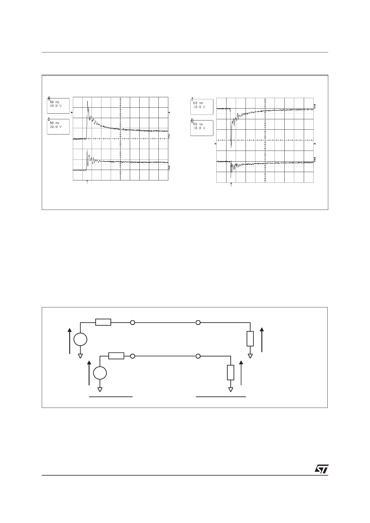
Figure 8. Remaining voltage at both stages S1 (Vinput) and S2 (Voutput) during
ESD surge
Vin
Vout
Vin
Vout
Positive surge
Negative surge
Please note that the USBUFxxW6 is not only acting for positive ESD surges but also for
negative ones. For these kinds of disturbances it clamps close to ground voltage as
shown in Figure 8. (negative surge.
2.4
Latch-up phenomena
The early ageing and destruction of IC’s is often due to latch-up phenomenon which is
mainly induced by dV/dt. Thanks to its structure, the USBUFxxW6 provides a high immunity
to latch-up phenomenon by smoothing very fast edges.
2.5
Crosstalk behavior
Figure 9.
Crosstalk phenomenon.
RG1
Line 1
VG1
RG2
Line 2
VG2
RL1
α1 VG1 + β1 V2 G2
RL2
α2 VG2 + β2 V1 G1
DRIVERS
RECEIVERS
The crosstalk phenomenon is due to the coupling between 2 lines. The coupling factor (β12
or β21) increases when the gap across lines decreases, particularly in silicon dice. In the
example above the expected signal on load RL2 is α2VG2, in fact the real voltage at this point
has got an extra value β21VG1. This part of the VG1 signal represents the effect of the
crosstalk phenomenon of the line 1 on the line 2. This phenomenon has to be taken into
account when the drivers impose fast digital data or high frequency analog signals in the
disturbing line. The perturbed line will be more affected if it works with low voltage signal or
high load impedance (few kΩ).
6/11
Share Link: 