ADG1409YCPZ-REEL7(Rev0) データシートの表示(PDF) - Analog Devices
部品番号
コンポーネント説明
メーカー
ADG1409YCPZ-REEL7
(Rev.:Rev0)
(Rev.:Rev0)
Analog Devices

ADG1409YCPZ-REEL7 Datasheet PDF : 20 Pages
| |||
ADG1408/ADG1409
PIN CONFIGURATIONS AND FUNCTION DESCRIPTIONS
A0 1
EN 2
VSS 3
S1 4
S2 5
S3 6
S4 7
D8
16 A1
15 A2
ADG1408
TOP VIEW
(Not to Scale)
14 GND
13 VDD
12 S5
11 S6
10 S7
9 S8
Figure 2. ADG1408 Pin Configuration (TSSOP)
VSS 1
S1 2
S2 3
S3 4
PIN 1
INDICATOR
ADG1408
TOP VIEW
(Not to Scale)
12 GND
11 VDD
10 S5
9 S6
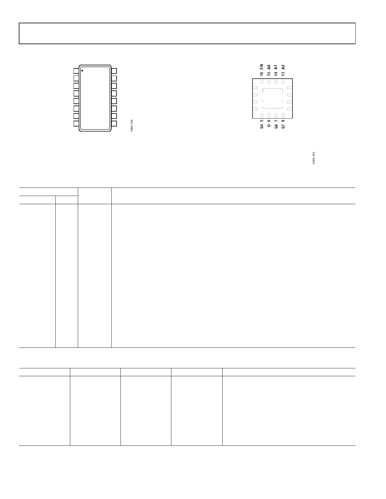
Figure 3. ADG1408 Pin Configuration (LFCSP_VQ),
Exposed Pad Tied to Substrate, VSS
Table 7. ADG1408 Pin Function Descriptions
Pin No.
TSSOP LFCSP_VQ Mnemonic Description
1
15
A0
Logic Control Input.
2
16
EN
Active High Digital Input. When low, the device is disabled and all switches are off. When high,
Ax logic inputs determine on switches.
3
1
VSS
Most Negative Power Supply Potential. In single supply applications, it can be connected
to ground.
4
2
S1
Source Terminal 1. Can be an input or an output.
5
3
S2
Source Terminal 2. Can be an input or an output.
6
4
S3
Source Terminal 3. Can be an input or an output.
7
5
S4
Source Terminal 4. Can be an input or an output.
8
6
D
Drain Terminal. Can be an input or an output.
9
7
S8
Source Terminal 8. Can be an input or an output.
10
8
S7
Source Terminal 7. Can be an input or an output.
11
9
S6
Source Terminal 6. Can be an input or an output.
12
10
S5
Source Terminal 5. Can be an input or an output.
13
11
VDD
Most Positive Power Supply Potential.
14
12
GND
Ground (0 V) Reference.
15
13
A2
Logic Control Input.
16
14
A1
Logic Control Input.
Table 8. ADG1408 Truth Table
A2
A1
A0
EN
ON SWITCH
X
X
X
0
NONE
0
0
0
1
1
0
0
1
1
2
0
1
0
1
3
0
1
1
1
4
1
0
0
1
5
1
0
1
1
6
1
1
0
1
7
1
1
1
1
8
Rev. 0 | Page 10 of 20
Share Link: