ADMC200 データシートの表示(PDF) - Analog Devices
部品番号
コンポーネント説明
メーカー
ADMC200 Datasheet PDF : 12 Pages
| |||
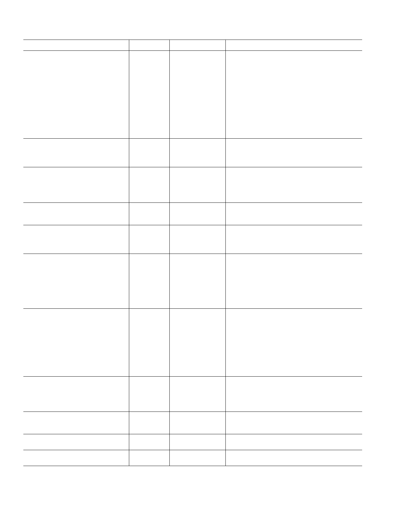
ADMC200–SPECIFICATIONS (VDD = +5 V ؎ 5%; AGND = DGND = 0 V; REFIN = 2.5 V; External Clock =
12.5 MHz; TA = –40؇C to +85؇C unless otherwise noted)
Parameter
ADMC200AP Units
Conditions/Comments
ANALOG-TO-DIGITAL CONVERTER1
Resolution
11
Relative Accuracy
±2
Differential Nonlinearity
±2
Bias Offset Error
±5
Bias Offset Match
4
Full-Scale Error
±6
Full-Scale Error Match
4
Conversion Time/Channel
40
Signal-to-Noise Ratio (SNR)2
60
Channel-to-Channel Isolation
Two-/Three-Phase Mode
–58
Three-/Three-Phase Mode
–55
ANALOG INPUTS
Input Voltage Level
0–5
Analog Input Current
100
Input Capacitance
10
TRACK AND HOLD
Aperture Delay
200
Aperture Time Delay Match
20
SHA Acquisition Time
20
Droop Rate
5
REFERENCE INPUT
Voltage Level
2.5
Reference Input Current
50
REFERENCE OUTPUT
Voltage Level
Voltage Level Tolerance
Drive Capability
2.5
±5
± 200
LOGIC
VIL
0.8
VIH
2.0
VOL
0.4
VOH
4.5
Input Leakage Current
1
Three-State Leakage Current
1
Input Capacitance
20
PWM TIMERS
Resolution
Programmable Deadtime Range
Programmable Deadtime Increments
Programmable Pulse Deletion Range
Programmable Deletion Increments
Minimum PWM Frequency
12
0–10.08
2
0–10.16
1
1.5
VECTOR TRANSFORMATION
Radius Error
Angular Error
Reverse Transformation Time
Forward Transformation Time
EXTERNAL CLOCK INPUT
Range
0.7
30
37
40
6.25–25
INTERNAL SYSTEM CLOCK
Range
POWER SUPPLY CURRENT
IDD
NOTES
1Measurements made with external reference.
2Tested with PWM Switching Frequency of 25 kHz.
Specifications subject to change without notice.
6.25–12.5
20
Bits
LSB max
LSB max
LSB max
LSB max
LSB max
LSB max
System CLK Cycles
dB min
dB max
dB max
Twos Complement Data Format
Integral Nonlinearity
Any Channel
Between Channels
Any Channel
Between Channels
fIN = 600 Hz Sine Wave, fSAMPLE = 55 kHz, 600 Hz
Sine Wave Applied to Unselected Channels
Volts
µA max
pF typ
ns max
ns max
System CLK Cycles
mV/ms max
Any Channel
Between Channels
V dc
µA max
Volts
% max
µA max
Full Load
V max
V min
V max
V min
µA max
µA max
pF typ
ISINK = 400 µA, VDD = 5 V
ISOURCE = 20 µA, VDD = 5 V
Bits
µs
System CLK Cycles
µs
System CLK Cycle
kHz
% max
arc min max
System CLK Cycles
System CLK Cycles
160 ns
80 ns
Resolution Varies with PWM Switching Frequency
(10 MHz Clock: 20 kHz = 9 Bits, 10 kHz = 10 Bits,
5 kHz = 11 Bits, 2.5 kHz = 12 Bits). Higher Fre-
quencies are Available with Lower Resolution
Park & Clarke Transformation
MHz
If > 12.5 MHz, Then It Is Necessary to Divide Down
via SYSCTRL Register
MHz
mA max
–2–
REV. B
Share Link: 