80C196KC データシートの表示(PDF) - Rochester Electronics
部品番号
コンポーネント説明
メーカー
80C196KC Datasheet PDF : 26 Pages
| |||
8XC196KC/8XC196KC20
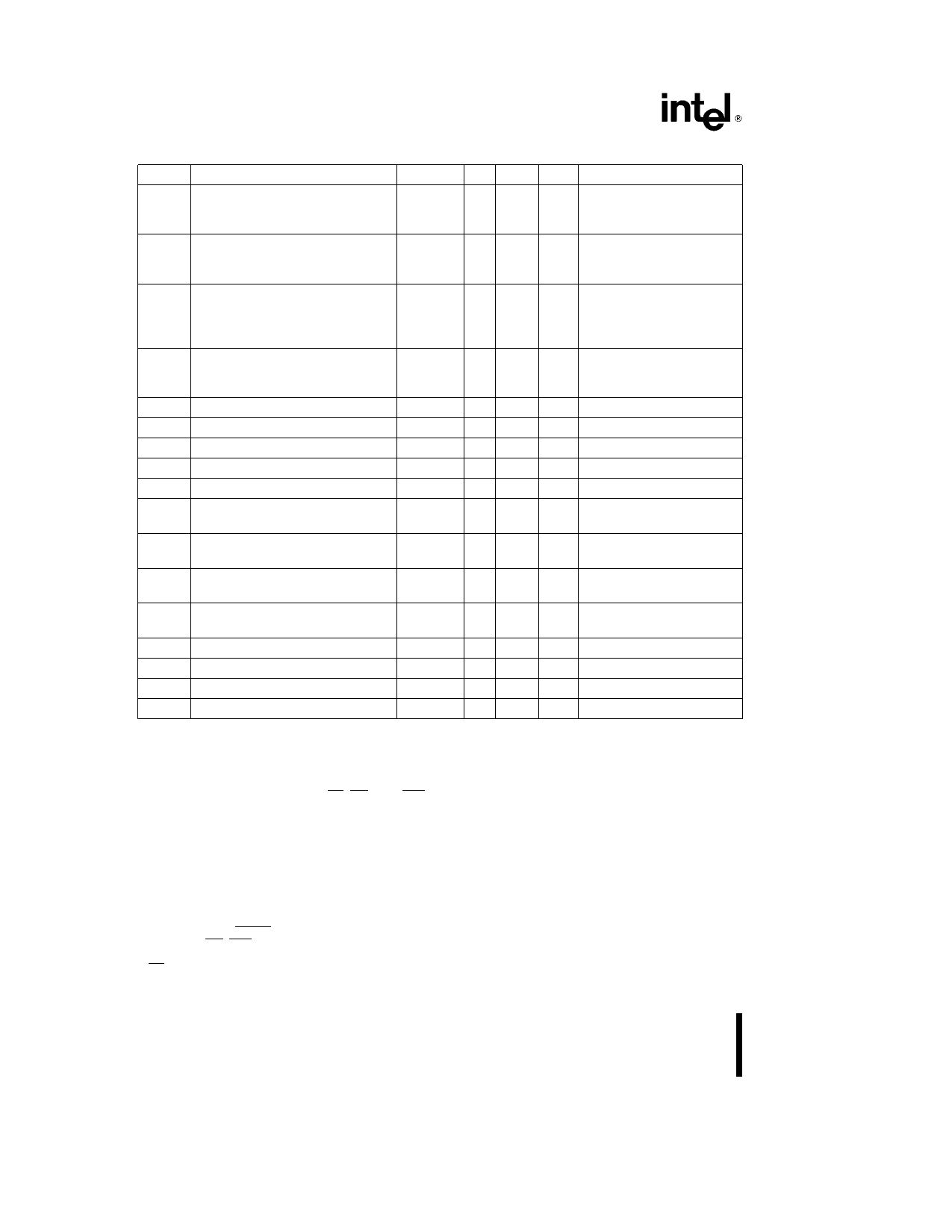
DC CHARACTERISTICS (Over Specified Operating Conditions) (Continued)
Symbol Description
Min
Typ Max Units TestConditions
VOH1
IOH1
Output High Voltage
(Quasi-bidirectional Outputs)
Logical 1 Output Current in Reset.
on P2.0. Do not exceed this
or device may enter test modes.
VCC b 0.3
VCC b 0.7
VCC b 1.5
b0.8
V IOH e b10 mA
V IOH e b30 mA
V IOH e b60 mA
mA VIH e VCC b 1.5V
IIL2
Logical 0 Input Current in Reset
on P2.0. Maximum current that
must be sunk by external
device to ensure test mode entry.
IIH1
Logical 1 Input Current.
Maximum current that external
device must source to initiate NMI.
TBD mA VIN e 0.45V
a200 mA VIN e VCC e 2.4V
ILI
ILI1
ITL
IIL
IIL1
ICC
ICC
IIDLE
Input Leakage Current (Std. Inputs)
Input Leakage Current (Port 0)
1 to 0 Transition Current (QBD Pins)
Logical 0 Input Current (QBD Pins)
Ports 3 and 4 in Reset
Active Mode Current in Reset
(8XC196KC)
Active Mode Current in Reset
(8XC196KC20)
Idle Mode Current (8XC196KC)
IIDLE Idle Mode Current (8XC196KC20)
IPD
Powerdown Mode Current
IREF A/D Converter Reference Current
RRST Reset Pullup Resistor
6K
CS
Pin Capacitance (Any Pin to VSS)
g10 mA 0 k VIN k VCC b 0.3V
g3 mA 0 k VIN k VREF
b650 mA VIN e 2.0V
b70 mA VIN e 0.45V
b70 mA VIN e 0.45V
65 75 mA XTAL1 e 16 MHz
VCC e VPP e VREF e 5.5V
80 92 mA XTAL1 e 20 MHz
VCC e VPP e VREF e 5.5V
17 25 mA XTAL1 e 16 MHz
VCC e VPP e VREF e 5.5V
21 30 mA XTAL1 e 20 MHz
VCC e VPP e VREF e 5.5V
8 15 mA VCC e VPP e VREF e 5.5V
2
5
mA VCC e VPP e VREF e 5.5V
65K X VCC e 5.5V, VIN e 4.0V
10 pF
NOTES:
1. All pins except RESET and XTAL1.
2. Violating these specifications in Reset may cause the part to enter test modes.
3. Commercial specifications apply to express parts except where noted.
4. QBD (Quasi-bidirectional) pins include Port 1, P2.6 and P2.7.
5. Standard Outputs include AD0±15, RD, WR, ALE, BHE, INST, HSO pins, PWM/P2.5, CLKOUT, RESET, Ports 3 and 4,
TXD/P2.0 and RXD (in serial mode 0). The VOH specification is not valid for RESET. Ports 3 and 4 are open-drain outputs.
6. Standard Inputs include HSI pins, READY, BUSWIDTH, RXD/P2.1, EXTINT/P2.2, T2CLK/P2.3 and T2RST/P2.4.
7. Maximum current per pin must be externally limited to the following values if VOL is held above 0.45V or VOH is held
below VCC b 0.7V:
IOL on Output pins: 10 mA
IOH on quasi-bidirectional pins: self limiting
IOH on Standard Output pins: 10 mA
8. Maximum current per bus pin (data and control) during normal operation is g3.2 mA.
9. During normal (non-transient) conditions the following total current limits apply:
Port 1, P2.6
HSO, P2.0, RXD, RESET
P2.5, P2.7, WR, BHE
AD0 ± AD15
RD, ALE, INST±CLKOUT
IOL: 29 mA
IOL: 29 mA
IOL: 13 mA
IOL: 52 mA
IOL: 13 mA
IOH is self limiting
IOH: 26 mA
IOH: 11 mA
IOH: 52 mA
IOH: 13 mA
10
Share Link: 