AS4C1M16E5 „Éá„Éľ„āŅ„ā∑„Éľ„Éą„ĀģŤ°®Á§ļÔľąPDFÔľČ - Alliance Semiconductor
ťÉ®ŚďĀÁē™ŚŹ∑
„ā≥„É≥„ÉĚ„Éľ„Éć„É≥„ÉąŤ™¨śėé
„É°„Éľ„āę„Éľ
AS4C1M16E5 Datasheet PDF : 22 Pages
| |||
AS4C1M16E5
¬ģ
Functional description
The AS4C1M16E5 is a high performance 16-megabit CMOS Dynamic Random Access Memory (DRAM) organized as 1,048,576 words √ó 16
bits. The device is fabricated using advanced CMOS technology and innovative design techniques resulting in high speed, extremely low
power and wide operating margins at component and system levels. The Alliance 16Mb DRAM family is optimized for use as main memory
in personal and portable PCs, workstations, and multimedia and router switch applications.
The AS4C1M16E5 features hyper page mode operation where read and write operations within a single row (or page) can be executed at
very high speed by toggling column addresses within that row. Row and column addresses are alternately latched into input buffers using the
falling edge of RAS and xCAS inputs, respectively. Also, RAS is used to make the column address latch transparent, enabling application of
column addresses prior to xCAS assertion. The AS4C1M16E5 provides dual UCAS and LCAS for independent byte control of read and write
access.
Extended data out (EDO), also known as 'hyper-page mode,' enables high speed operation. In contrast to 'fast-page mode' devices, data
remains active on outputs after xCAS is de-asserted high, giving system logic more time to latch the data. Use OE and WE to control output
impedance and prevent bus contention during read-modify-write and shared bus applications. Outputs also go to high impedance at the last
occurrance of RAS and xCAS going high.
Refresh on the 1024 address combinations of A0 to A9 must be performed every 16 ms using:
‚ÄĘ RAS-only refresh: RAS is asserted while xCAS is held high. Each of the 1024 rows must be strobed. Outputs remain high impedence.
‚ÄĘ Hidden refresh: xCAS is held low while RAS is toggled. Outputs remain low impedence with previous valid data.
‚ÄĘ CAS-before-RAS refresh (CBR): At least one xCAS is asserted prior to RAS. Refresh address is generated internally.
Outputs are high-impedence (OE and WE are don't care).
‚ÄĘ Normal read or write cycles refresh the row being accessed.
The AS4C1M16E5 is available in the standard 42-pin plastic SOJ and 44/50-pin TSOP II packages, respectively. The AS4C1M16E5 device
operates with a single power supply of 5V ¬Ī 0.5V and provides TTL compatible inputs and outputs.
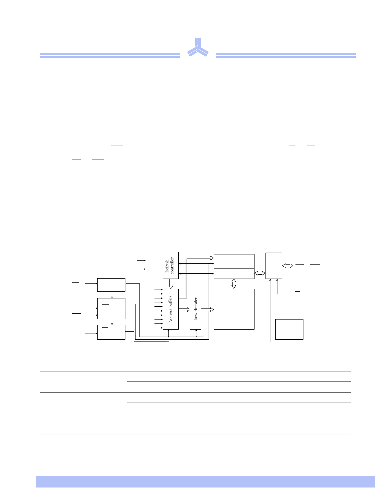
Logic block diagram
RAS
UCAS
LCAS
WE
VCC
GND
RAS clock
generator
A0
A1
A2
A3
CAS clock
A4
generator
A5
A6
A7
A8
WE clock
A9
generator
Column decoder
Sense amp
Data
DQ
buffers
DQ1 to DQ16
1024 √ó 1024 √ó 16
Array
(16,777,216)
OE
Substrate bias
generator
Recommended operating conditions
Parameter
Symbol
Min
Supply voltage
VCC
4.5
GND
0.0
Input voltage
VIH
2.4
VIL
‚Äď0.5‚Ć
Commercial
Ambient operating temperature
Industrial
0
TA
-40
†VIL min -3.0V for pulse widths less than 5 ns.
Recommended operating conditions apply throughout this document unless otherwise specified.
Nominal
5.0
0.0
‚Äď
‚Äď
‚Äď
‚Äď
Max Unit
5.5
V
0.0
V
VCC
V
0.8
V
70
¬įC
85
4/11/01; v.1.0
Alliance Semiconductor
P. 2 of 22
Share Link: 