BCR16CM-12LA データシートの表示(PDF) - Renesas Electronics
部品番号
コンポーネント説明
メーカー
BCR16CM-12LA Datasheet PDF : 7 Pages
| |||
BCR16CM-12LA
Parameter
RMS on-state current
Surge on-state current
I2t for fusing
Peak gate power dissipation
Average gate power dissipation
Peak gate voltage
Peak gate current
Junction temperature
Storage temperature
Mass
Notes: 1. Gate open.
Symbol
IT (RMS)
ITSM
I2t
PGM
PG (AV)
VGM
IGM
Tj
Tstg
—
Ratings
16
170
121
5.0
0.5
10
2
– 40 to +125
– 40 to +125
2.0
Unit
Conditions
A
Commercial frequency, sine full wave
360°conduction, Tc = 100°CNote3
A
60Hz sinewave 1 full cycle, peak value,
non-repetitive
A2s
Value corresponding to 1 cycle of half
wave 60Hz, surge on-state current
W
W
V
A
°C
°C
g
Typical value
Electrical Characteristics
Parameter
Symbol Min.
Typ.
Max.
Unit
Test conditions
Repetitive peak off-state current
IDRM
—
On-state voltage
VTM
—
Gate trigger voltageNote2
Ι
VFGTΙ
—
ΙΙ
VRGTΙ
—
ΙΙΙ
VRGTΙΙΙ
—
Gate trigger currentNote2
Ι
IFGTΙ
—
ΙΙ
IRGTΙ
—
ΙΙΙ
IRGTΙΙΙ
—
—
2.0
mA Tj = 125°C, VDRM applied
—
1.5
V
Tc = 25°C, ITM = 25 A,
Instantaneous measurement
—
1.5
V
Tj = 25°C, VD = 6 V, RL = 6 Ω,
—
1.5
V
RG = 330 Ω
—
1.5
V
—
30Note6
mA Tj = 25°C, VD = 6 V, RL = 6 Ω,
—
30Note6
mA RG = 330 Ω
—
30Note6
mA
Gate non-trigger voltage
Thermal resistance
VGD
0.2
—
—
V
Tj = 125°C, VD = 1/2 VDRM
Rth (j-c)
—
—
1.4
°C/W Junction to caseNote3 Note4
Critical-rate of rise of off-state
(dv/dt)c
10
—
—
V/µs Tj = 125°C
commutating voltageNote5
Notes: 2. Measurement using the gate trigger characteristics measurement circuit.
3. Case temperature is measured at the T2 tab 1.5 mm away from the molded case.
4. The contact thermal resistance Rth (c-f) in case of greasing is 1.0°C/W.
5. Test conditions of the critical-rate of rise of off-state commutating voltage is shown in the table below.
6. High sensitivity (IGT ≤ 20 mA) is also available. (IGT item: 1)
Test conditions
1. Junction temperature
Tj = 125°C
2. Rate of decay of on-state commutating current
(di/dt)c = – 8.0 A/ms
3. Peak off-state voltage
VD = 400 V
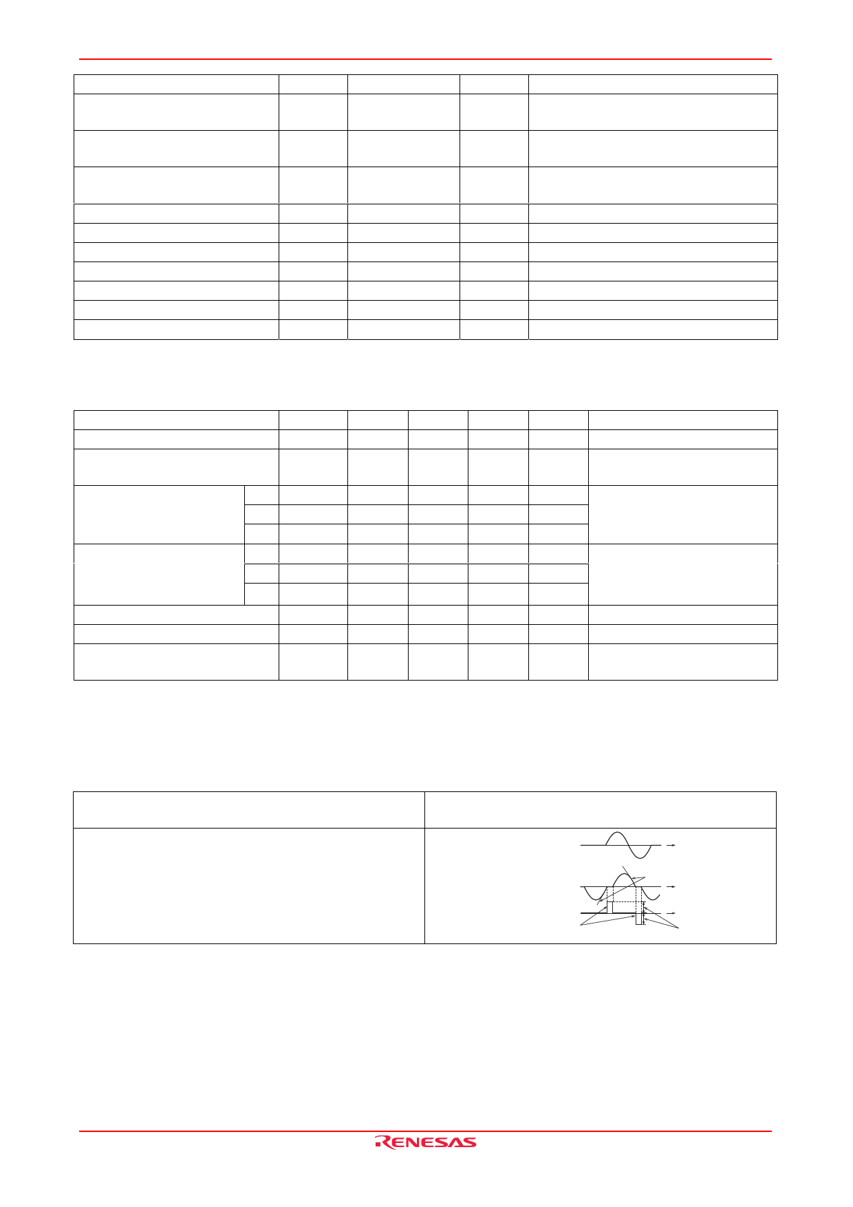
Commutating voltage and current waveforms
(inductive load)
Supply Voltage
Time
Main Current
Main Voltage
(dv/dt)c
(di/dt)c
Time
Time
VD
REJ03G0298-0300 Rev.3.00 Nov 30, 2007
Page 2 of 6
Share Link: 