BD3509MUV データシートの表示(PDF) - ROHM Semiconductor
部品番号
コンポーネント説明
メーカー
BD3509MUV Datasheet PDF : 21 Pages
| |||
BD3508MUV,BD3509MUV
Technical Note
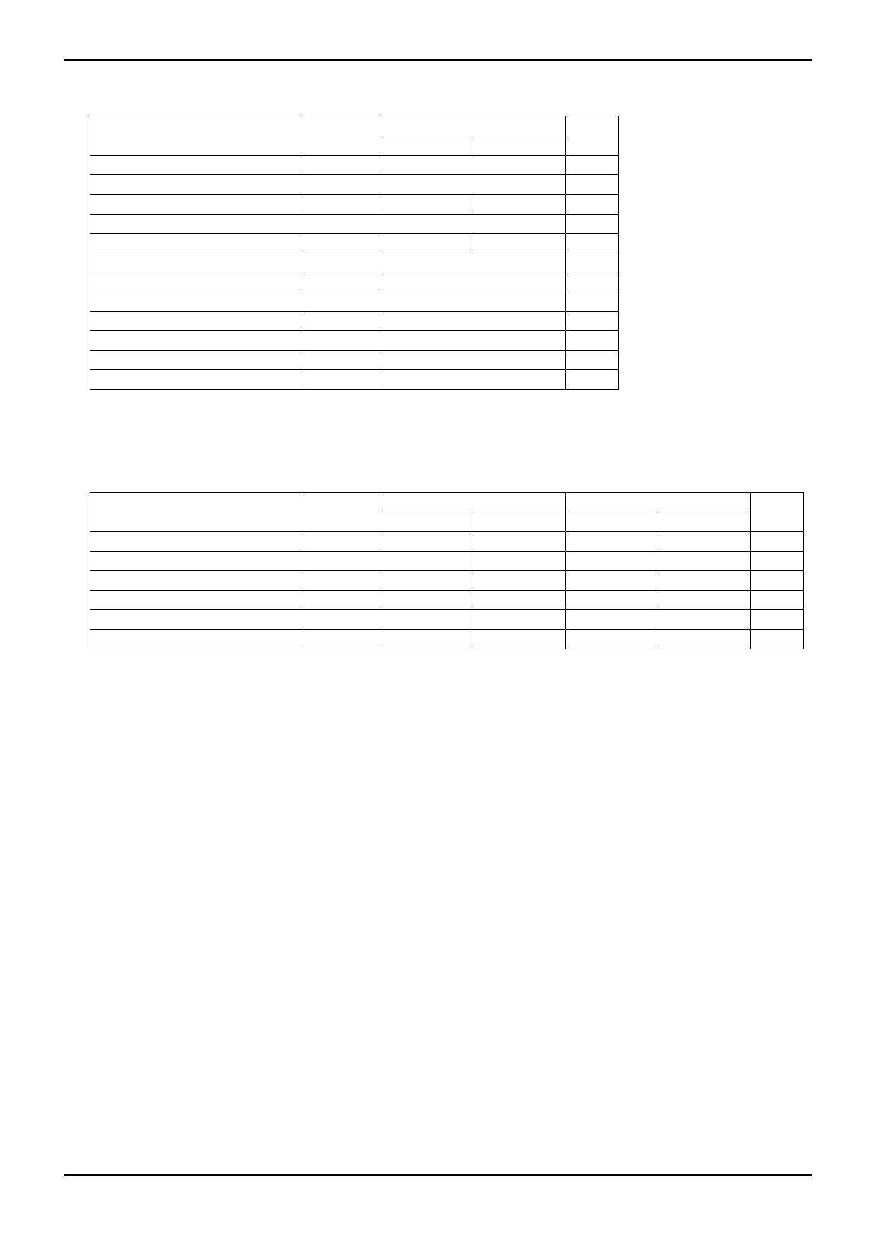
●Absolute Maximum Ratings (Ta=100℃)
BD3508MUV / BD3509MUV
Parameter
Input Voltage 1
Input Voltage 2
Input Voltage 3
Symbol
VCC
VIN
VDD
Ratings
BD3508MUV BD3509MUV
Unit
6.0 *1
V
6.0 *1
V
-
6.0*1
V
Enable Input Voltage
Ven
6.0
V
Power Good Input Voltage
Power Dissipation 1
Power Dissipation 2
Power Dissipation 3
Power Dissipation 4
VPGOOD
Pd1
Pd2
Pd3
Pd4
-
6.0
V
0.34 *2
W
0.70 *3
W
1.21 *4
W
3.56 *5
W
Operating Temperature Range
Topr
-10 ~ +100
℃
Storage Temperature Range
Tstg
-55 ~ +125
℃
Maximum Junction Temperature
Tjmax
+150
℃
*1 Should not exceed Pd.
*2 Reduced by 4mW/℃ for each increase in Ta≧25℃(no heat sink)
*3 1 layer, mounted on a board 74.2mm×74.2mm×1.6mm Glass-epoxy PCB (Copper foil area : 10.29mm2)
*4 4 layers, mounted on a board 74.2mm×74.2mm×1.6mm Glass-epoxy PCB (Copper foil area : 10.29mm2) , copper foil in each layers.
*5 4 layers, mounted on a board 74.2mm×74.2mm×1.6mm Glass-epoxy PCB (Copper foil area : 5505mm2) , copper foil in each layers.
●Operating Conditions(Ta=25℃)
Parameter
Symbol
BD3508MUV
Min
Max
Input Voltage 1
Input Voltage 2
VCC
VIN
4.3
5.5
0.75
VCC-1 *6
Input Voltage 3
VDD
-
-
Output Voltage setting Range
Vo
VFB
2.7
Enable Input Voltage
Ven
-0.3
5.5
NRCS capacity
CNRCS
0.001
1
*6 VCC and VIN do not have to be implemented in the order listed.
★This product is not designed for use in radioactive environments.
BD3509MUV
Min
Max
Unit
4.3
5.5
V
0.7
VCC-1 *6
V
2.7
5.5
V
VFB
2.7
V
-0.3
5.5
V
0.001
1
µF
www.rohm.com
© 2010 ROHM Co., Ltd. All rights reserved.
2/20
2010.04 - Rev.C
Share Link: 