BGD712C(2007) データシートの表示(PDF) - NXP Semiconductors.
部品番号
コンポーネント説明
メーカー
BGD712C Datasheet PDF : 7 Pages
| |||
NXP Semiconductors
BGD712C
750 MHz, 18.5 dB gain power doubler amplifier
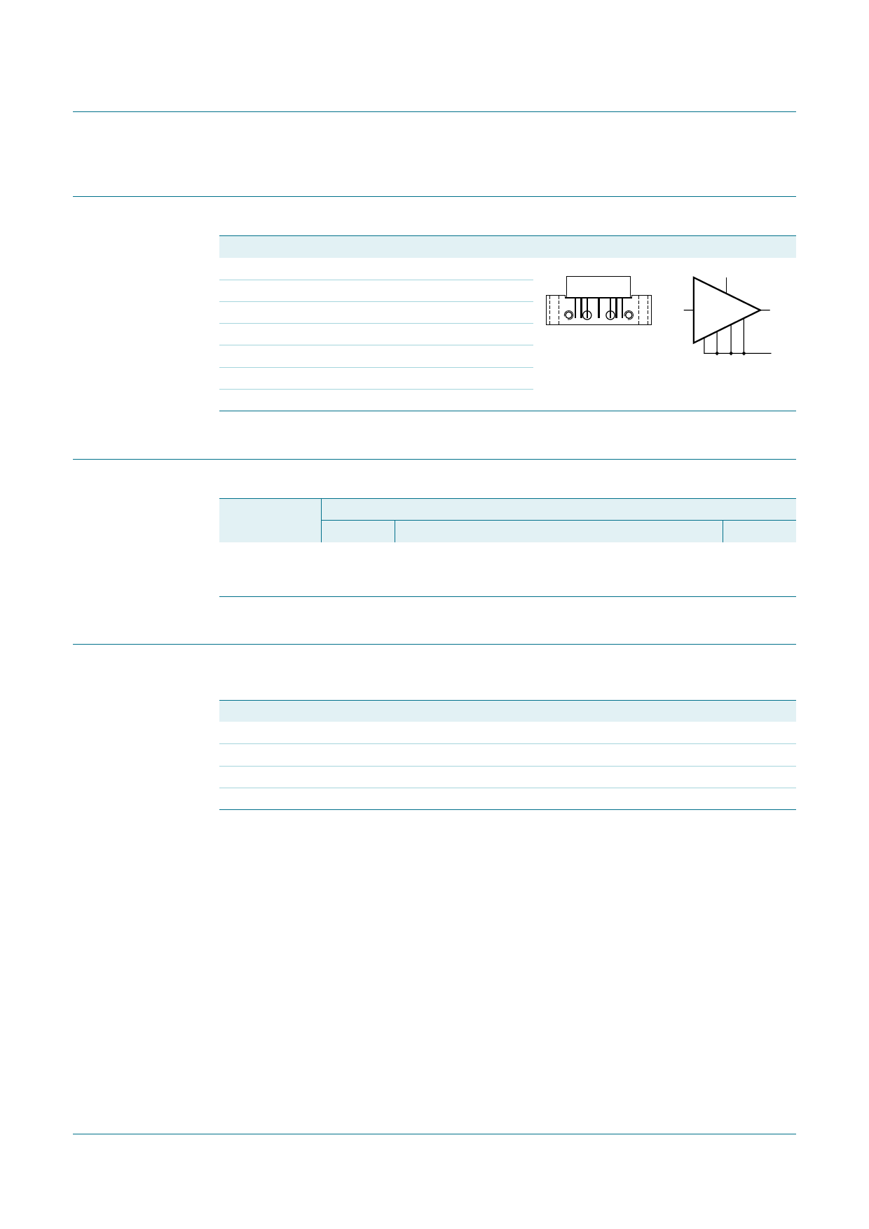
2. Pinning information
Table 2:
Pin
1
2
3
5
7
8
9
Pinning
Description
input
common
common
+VB
common
common
output
Simplified outline Symbol
13579
5
1
9
23 78
sym095
3. Ordering information
Table 3: Ordering information
Type number Package
Name
Description
BGD712C
-
rectangular single-ended package; aluminium flange;
2 vertical mounting holes; 2 × 6-32 UNC and 2 extra
horizontal mounting holes; 7 gold-plated in-line leads
Version
SOT115J
4. Limiting values
Table 4: Limiting values
In accordance with the Absolute Maximum Rating System (IEC 60134).
Symbol Parameter
Conditions
Min
VB
supply voltage
-
Vi
input voltage
-
Tstg
storage temperature
−40
Tmb
mounting base temperature
−20
Max
30
70
+100
+100
Unit
V
dBmV
°C
°C
BGD712C_2
Product data sheet
Rev. 02 — 16 August 2007
© NXP B.V. 2007. All rights reserved.
2 of 7
Share Link: 